Printed wiring board including power supply layer and ground layer

a technology of printed wiring and ground layer, which is applied in the field of printed wiring boards, can solve the problems of forced pass through the electrically-conductive pieces of power supply noise and forced current to force through the electrically-conductive pieces

Active Publication Date: 2008-09-23
FUJITSU LTD
View PDF6 Cites 18 Cited by
  • Summary
  • Abstract
  • Description
  • Claims
  • Application Information

AI Technical Summary

Benefits of technology

[0006]It is accordingly an object of the present invention to provide a printed wiring board capable of reliably reducing power supply noise.
[0009]The first electrically-conductive piece serves to narrow the path of electric current from the first electrically-conductive power supply layer to the second electrically-conductive power supply layer. The second electrically-conductive piece likewise serves to narrow the path of electric current from the second electrically-conductive ground layer to the first electrically-conductive ground layer. Noise in the electric current, namely power supply noise is forced to inevitably pass through the electrically-conductive pieces. The power supply noise thus reliably flows into the capacitor through the first and second electrically-conductive pieces. The printed wiring board is in this manner allowed to enjoy a sufficient suppression of the power supply noise. Electromagnetic waves are reliably prevented from radiation from the printed wiring board. The second electrically-conductive piece may preferably be contoured at least partly based on a projected image of the first electrically-conductive piece.
[0010]The first electrically-conductive piece may be connected to the second electrically-conductive power supply layer at a position closer to a clock terminal of the electronic circuit element. Likewise, the second electrically-conductive piece is connected to the second electrically-conductive ground layer at a position closer to a clock terminal of the electronic circuit element. The return current of a clock signal is thus allowed to circulate in the shortest path. The waveform is prevented from deformation in the clock signal. Noise can surely be suppressed. The printed wiring board is allowed to enjoy a suppressed radiation of electromagnetic waves resulting from the clock signal.
[0012]The combination of the first and second electrically-conductive power supply layers and the first electrically-conductive piece and the combination of the first and second electrically-conductive ground layers and the second electrically-conductive piece may alternately be layered on one another in the printed wiring board. Such a layered structure serves to enhance the interlayer capacitance between the island of the second electrically-conductive power supply layer and the island of the second electrically-conductive ground layer. This increase in the capacitance serves to enhance reduction of power supply noise.
[0013]The first electrically-conductive ground layer may at least partly overlap a projected image of the second electrically-conductive power supply layer. This results in establishment of an electrostatic coupling of a smaller capacitance between the first electrically-conductive ground layer and the second electrically-conductive power supply layer. The electrostatic coupling serves to suppress deformation of waveform in a signal of the gigahertz unit.
[0015]Otherwise, the printed wiring board may further comprise: a third insulating layer; a third electrically-conductive ground layer formed on the surface of the third insulating layer; an island of a fourth electrically-conductive ground layer contoured based on a projected image of the electronic circuit element, the fourth electrically-conductive ground layer isolated from the third electrically-conductive ground layer on the surface of the third insulating layer; a third electrically-conductive piece connecting the fourth electrically-conductive ground layer to the third electrically-conductive ground layer; and vias connecting the second and fourth electrically-conductive ground layers to each other at positions outside the second electrically-conductive power supply layer located in a space between the second and fourth electrically-conductive ground layers. The vias function as a shield for the island of the second electrically-conductive power supply layer. This results in a significant reduction of radiation of electromagnetic waves from the second electrically-conductive power supply layer.

Problems solved by technology

Noise in the electric current, namely power supply noise is forced to inevitably pass through the electrically-conductive pieces.

Method used


Image

  • Printed wiring board including power supply layer and ground layer
  • Printed wiring board including power supply layer and ground layer
  • Printed wiring board including power supply layer and ground layer

Examples


Embodiment Construction

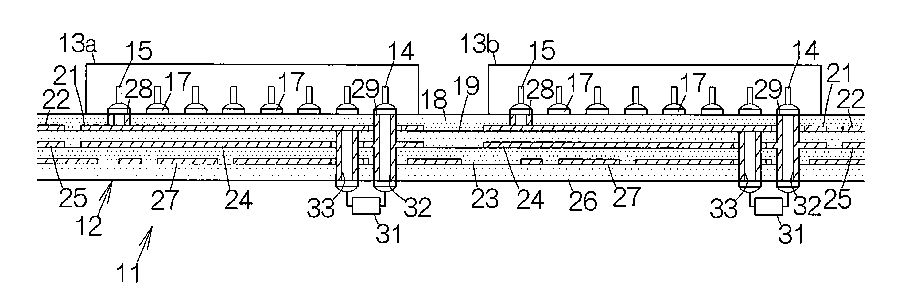
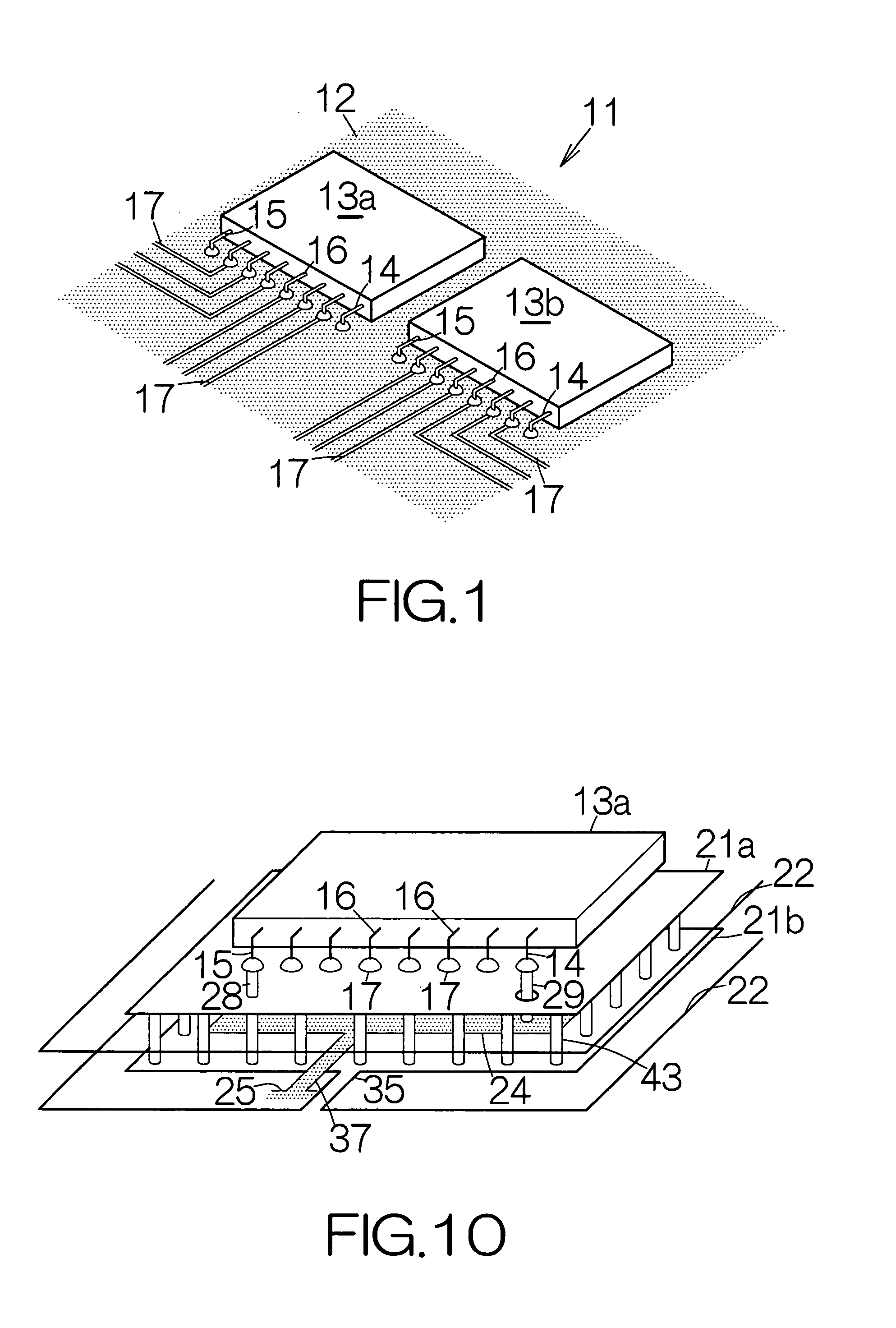
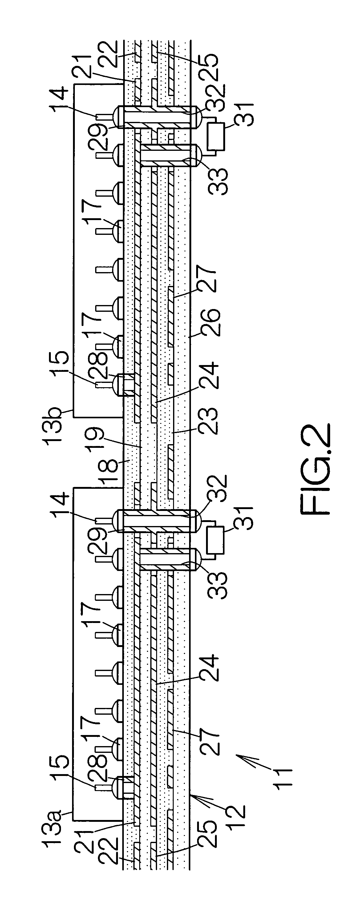
[0027]FIG. 1 schematically illustrates a printed circuit board unit 11 according to an embodiment of the present invention. The printed circuit board unit 11 includes a printed wiring board 12. One or more LSI (Large-Scale Integrated circuit) chip or chips 13a, 13b, . . . are mounted on the front surface of the printed wiring board 12, for example. A power supply pin 14, a ground pin 15 and signal pins 16 are connected to each of the LSI chips 13a, 13b.

[0028]Wiring patterns 17 are formed on the surface of the printed wiring board 12. The wiring patterns 17 may be made of an electrically-conductive material such as copper, for example. The signal pins 16 are soldered to the corresponding wiring patterns 17, respectively.

[0029]As shown in FIG. 2, the wiring patterns 17 are received on the uppermost layer of the printed wiring board 12, namely the upper surface of a first insulating layer 18. The first insulating layer 18 is received on the upper surface of a second insulating layer 1...


PUM


Abstract

A first power supply layer spreads over an insulating layer outside an island of a second power supply layer. A first ground layer spreads over an insulating layer outside an island of a second ground layer. First and second electrically-conductive pieces are interposed between the first and second power supply layers as well as between the first and second ground layers. A capacitor is interposed between the first and second electrically-conductive pieces. Power supply noise is forced to inevitably pass through the electrically-conductive pieces. The power supply noise thus reliably flows into the capacitor through the first and second electrically-conductive pieces. A printed wiring board is in this manner allowed to enjoy a sufficient suppression of the power supply noise.

Description

BACKGROUND OF THE INVENTION[0001]1. Field of the Invention[0002]The present invention relates to a printed wiring board including an electrically-conductive power supply layer and an electrically-conductive ground layer.[0003]2. Description of the Prior Art[0004]A printed wiring board usually includes an electrically-conductive power supply layer and an electrically-conductive ground layer. A LSI (Large-Scale Integrated circuit) chip is mounted on the surface of the printed wiring board. The LSI chip is connected to the electrically-conductive power supply layer and the electrically-conductive ground layer. A chip capacitor, namely a bypass capacitor, is connected to the electrically-conductive power supply layer and the electrically-conductive ground layer. The bypass capacitor serves to reduce power supply noise.[0005]Japanese Patent Application Publication Nos. 6-244562 and 11-233951 disclose an island of an electrically-conductive power supply layer and an island of an electrica...

Claims


Application Information

Patent Timeline
Patent Type & Authority Patents(United States)
IPC IPC(8): H05K1/11H05K1/14
CPCH05K1/0225H05K1/0231H05K1/0298H05K2201/10689H05K2201/09309H05K2201/09663H05K2201/10545H05K2201/093
Inventor NAKAO, TOMOYUKI
Owner FUJITSU LTD
Why Eureka
Try Eureka