Apparatus and method for bonding silicon wafer to conductive substrate

a technology of silicon wafers and substrates, applied in the direction of basic electric elements, sustainable manufacturing/processing, final product manufacturing, etc., can solve the problems of reducing the overall collection efficiency of dies, reducing the efficiency of conductive substrates, and limited dies b>200/b> that may be bonded to substrates

Inactive Publication Date: 2008-10-07
CYRIUM SOLAR
View PDF3 Cites 20 Cited by
  • Summary
  • Abstract
  • Description
  • Claims
  • Application Information

AI Technical Summary

Benefits of technology

[0012]The invention in one embodiment features a substrate having a first layer characterized by a first coefficient of thermal expansion (CTE), and a second layer characterized by a second CTE different than the first CTE, and a layer of solder adapted to bond the first layer to one or more semiconductor dies. The term die encompasses semiconductor wafers,

Problems solved by technology

The maximum size of a die 200 that may be bonded to a substrate is, however, generally limited due to the deformation of the die when subject to heat.
In addition to problems bonding large dies to substrate, the dies cut from wafers generally possess conducti

Method used


Image

  • Apparatus and method for bonding silicon wafer to conductive substrate
  • Apparatus and method for bonding silicon wafer to conductive substrate
  • Apparatus and method for bonding silicon wafer to conductive substrate

Examples


third embodiment

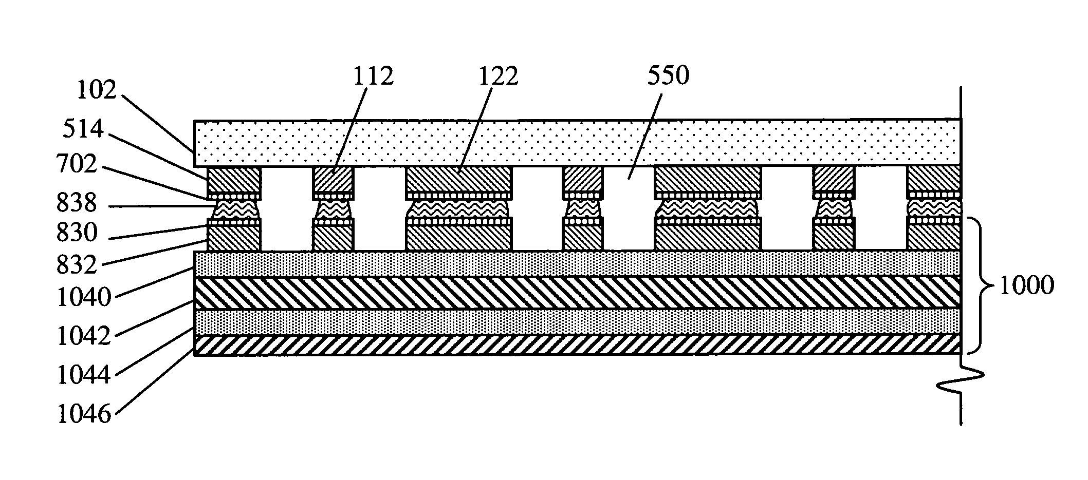
[0046]Illustrated in FIG. 10 is a sectional view of the photovoltaic die bonded to a complementary second substrate in accordance with a third preferred embodiment of the present invention. The invention in the third embodiment includes a third substrate 1000 that provides structural support for the die 600 while dissipating thermal energy received there from. Like the second substrate 800 described above, the third substrate 1000 also provides enhanced electrical conductivity to the embedded cross bars 112, 514, 122 of the die 600 and electrical coupling between the first set of traces 112, 514 and between the second set of traces 122. The conductive traces of the die 600 together with cross bars embedded in the substrate and solder there between cooperate to form a laminated power circuit (for internally collecting current within the die or solar panel) that substantially reduces resistive losses compared to prior art photovoltaic cells.

[0047]The first set of conductive structures...

fourth embodiment

[0055]Illustrated in FIG. 11 is a side view of a heat sink adapted to receive a die and substrate, in accordance with a The combination of die 600 and first substrate 800 or second substrate 1000, for example, may be bonded to the heat sink 1102 using elastomeric, thermally conductive material such as a phase changer thermal compound. Some phase changer thermal compounds well known to those skilled in the art are pressure sensitive and have optimum thermal conductive properties when subjected to elevated pressure. This increased pressure may be achieved by securing a die 600 and substrate 1000 having a predetermined curvature within a heatsink in a manner that allows in the curvature to bias at least a portion of the substrate onto the heatsink.

[0056]In the third preferred embodiment discussed above, the composition and thickness of the plurality of plies of the substrate 1000 are selected to induce a curvature in the first ply 832 that is substantially equal to the curvature of th...


PUM

PropertyMeasurementUnit
Temperatureaaaaaaaaaa
Thicknessaaaaaaaaaa
Electrical conductivityaaaaaaaaaa

Abstract

A system and method is disclosed for bonding a substrate to a semiconductor die that is prone to curling when subjected to an elevated temperature in a solder reflow oven, for example, thereby improving the electrical and mechanical bonding for large dies, wafers, chips, and photovoltaic cells. In one embodiment, the substrate is adapted to curl to the same degree as the die to form a uniform gap between the substrate and die across the boundary there between. In another embodiment, solder used to bond the die and substrate is applied such that the volume deposited varies based on the expected gap between the die and substrate when heated to the melting temperature of the solder.

Description

CROSS-REFERENCE TO RELATED APPLICATION[0001]This application claims priority from the following U.S. Provisional Patent Application, the disclosure of which is hereby incorporated herein by reference in its entirety for all purposes: U.S. Provisional Patent Application Ser. No. 60 / 618,368, to Gregory Alan Bone, entitled “Apparatus and Method for Bonding Silicon Wafer to Patterned Conductive Substrate,” filed Oct. 12, 2004.BACKGROUND[0002]Solar cells, also known as photovoltaic cells, for converting light into electricity are becoming an increasingly viable source of power when compared to traditional petroleum based sources of energy. Solar cells come in many types including monocrystalline, polycrystalline, and thin-film. Some of the most efficient solar cells, e.g., monocrystalline cells, are thin slices called wafers that are cut from a single silicon crystal produced in the form of an ingot. The silicon may be doped with select impurities to form two separate semiconductor struc...

Claims


Application Information

Patent Timeline
IPC IPC(8): H01L23/48
CPCH01L24/17H01L25/0655H01L31/0516H01L31/1804H01L23/367Y10T29/49144H01L24/14H01L24/16H01L24/73H01L24/81H01L2224/05611H01L2224/0603H01L2224/13099H01L2224/1403H01L2224/16238H01L2224/1703H01L2224/73204H01L2224/81192H01L2224/81815H01L2924/01013H01L2924/01029H01L2924/1517H01L2924/3511H01L2924/01005H01L2924/01006H01L2924/01033H01L2924/01047H01L2924/014H01L2924/00013H01L24/13H01L2224/0401H01L2924/10253Y02E10/547H01L2224/29099H01L2924/00Y02P70/50
Inventor BONE, GREGORY ALAN
Owner CYRIUM SOLAR
Why Eureka
Try Eureka