Semiconductor integrated circuit

a technology of integrated circuits and semiconductors, applied in logic circuit coupling/interface arrangements, instruments, pulse techniques, etc., can solve the problems of reducing the power consumption of semiconductor devices, affecting the reliability of data held in logic circuits, and affecting the reliability of data retention, so as to reduce the leak current and simplify the circuit configuration. , the effect of reliably holding data

Active Publication Date: 2008-10-14
LAPIS SEMICON CO LTD
View PDF4 Cites 26 Cited by
  • Summary
  • Abstract
  • Description
  • Claims
  • Application Information

AI Technical Summary

Benefits of technology

[0008]With the foregoing in view, it is an object of the present invention to provide a semiconductor integrated circuit which is simple in circuit configuration and capable of reliably holding data in a standby mode and which is less reduced in leak current.
[0010]According to the present invention, a gate circuit is provided between a data non-holding circuit and a data holding circuit both corresponding to logic circuits, and an input signal value of the data holding circuit is fixed in a standby mode. Therefore, a semiconductor integrated circuit which is less reduced in leak current and capable of holding data therein in the standby mode, can be obtained with a simple circuit configuration.

Problems solved by technology

As one factor that will increase power consumption of the semiconductor device, there is known a leak current that flows through each of MOS transistors and diodes which constitute an integrated circuit.
However, the conventional MTCMOS technique is accompanied by a drawback that when the power switch (i.e., high threshold MOS transistor which performs connection / disconnection between the pseudo source line and the source line VDD) is turned off and thereby brought to the standby mode, data retained in the logic circuit is erased.
In this case, however, a new drawback occurs in that a circuit scale increases.
The conventional VTCMOS technique is accompanied by drawbacks that since the operating threshold values of all MOS transistors formed in the same substrate are simultaneously changed, the parasitic capacity becomes large and the time required to perform switching between the operation mode and the standby mode becomes longer.

Method used


Image

  • Semiconductor integrated circuit
  • Semiconductor integrated circuit
  • Semiconductor integrated circuit

Examples


first preferred embodiment

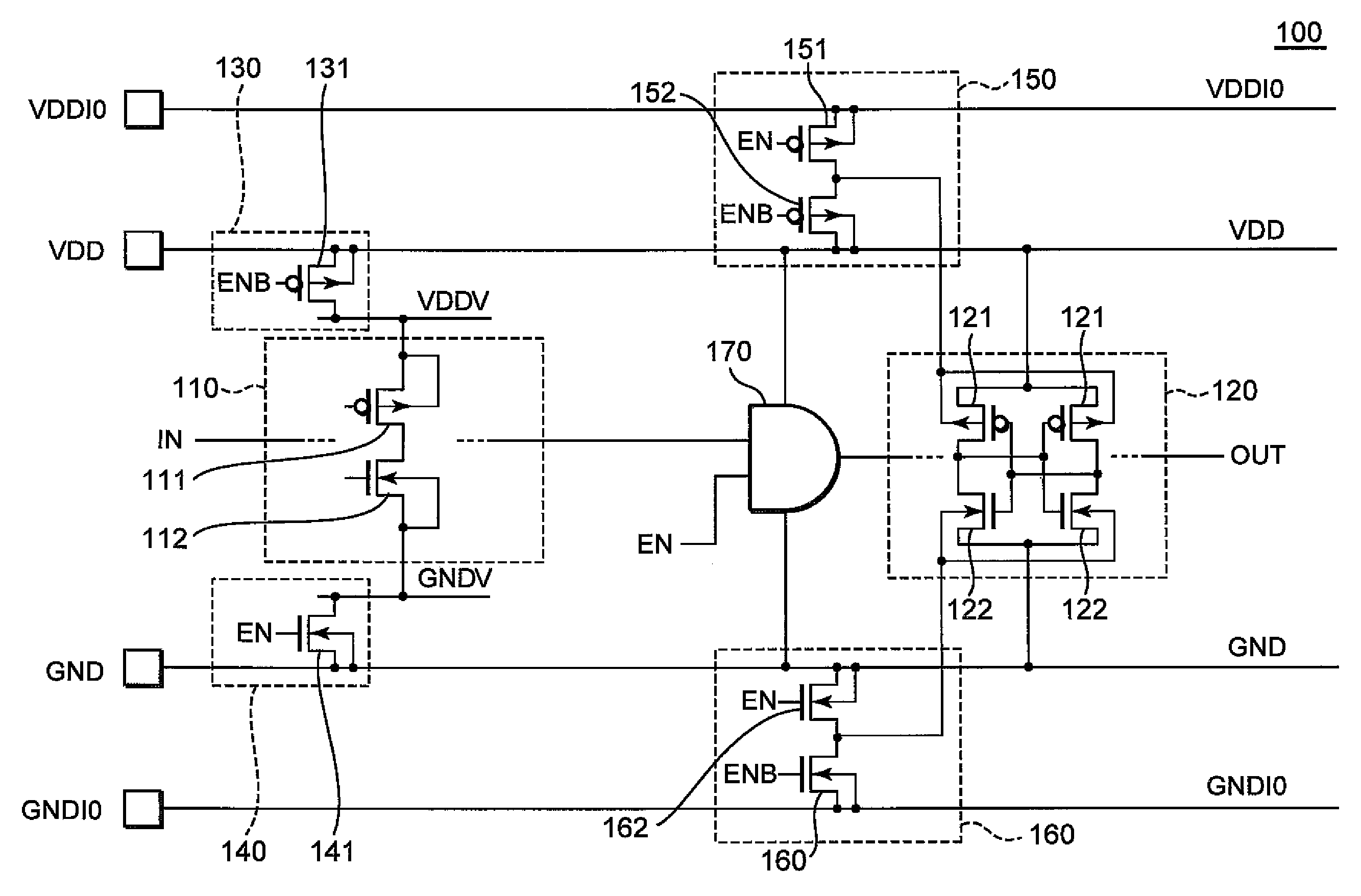
[0017]A semiconductor integrated circuit according to a first embodiment of the present invention will be explained below using FIG. 1.

[0018]As shown in FIG. 1, the semiconductor integrated circuit 100 according to the present embodiment comprises a data non-holding circuit 110, a data holding circuit 120, a virtual source line VDDV, a virtual ground line GNDV, a first source line VDD, a ground line GND, a second source line VDDIO, a second ground line GNDIO, switches 130, 140, 150 and 160 and a gate circuit 170.

[0019]The data non-holding circuit 110 is of a logic circuit that does not retain or hold data during a standby mode. The data non-holding circuit 110 is normally configured using a number of low threshold CMOS transistors (pMOS transistors 111 and nMOS transistors 112).

[0020]The data holding circuit 120 is of a logic circuit that needs to hold data during the standby mode. The data holding circuit is normally configured using a number of low threshold CMOS transistors (pMOS...

second preferred embodiment

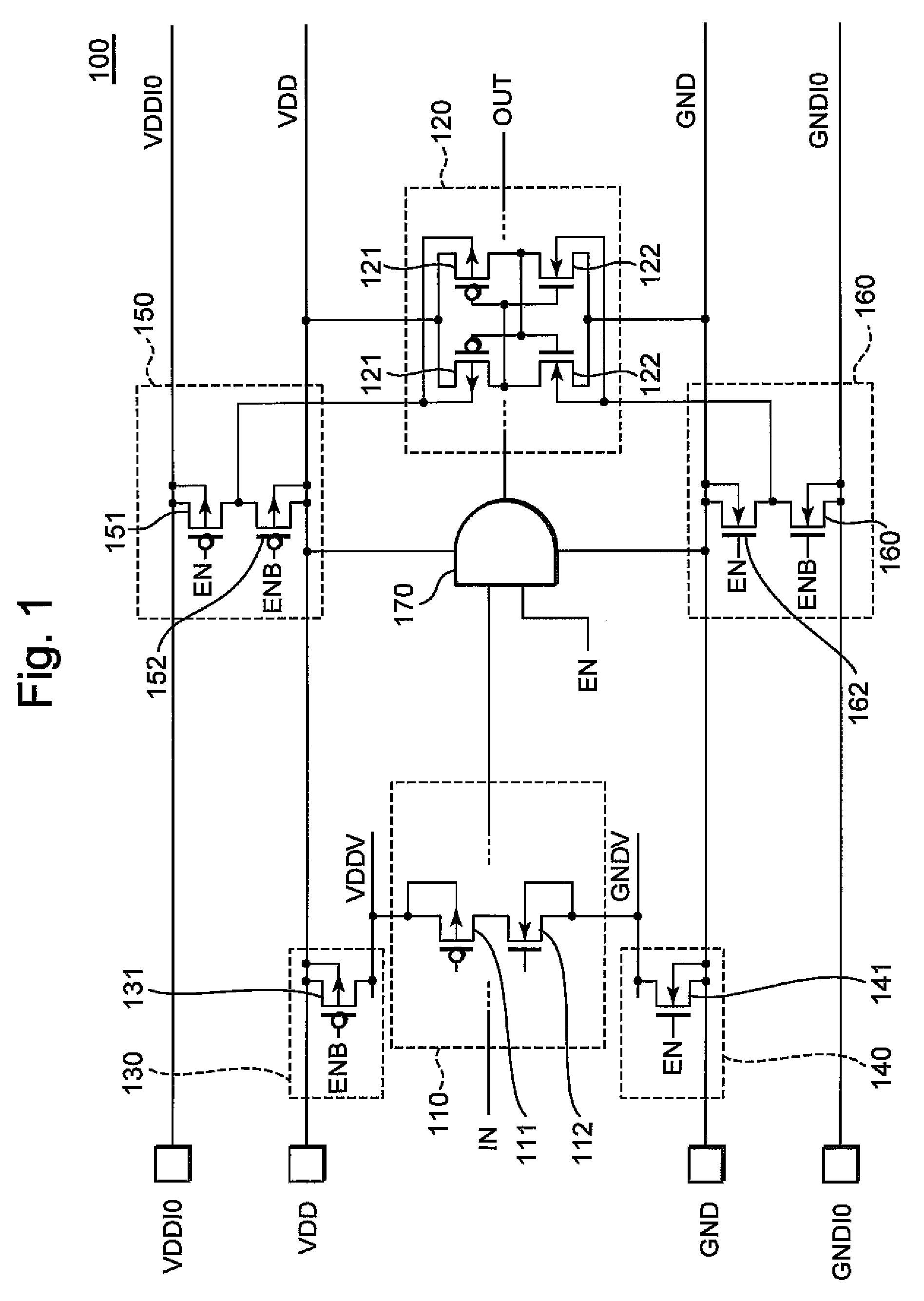
[0051]A semiconductor integrated circuit according to a second embodiment of the present invention will next be explained using FIG. 2.

[0052]In FIG. 2, constituent elements respectively given the same reference numbers as those in FIG. 1 respectively indicate ones identical to those shown in FIG. 1.

[0053]As shown in FIG. 2, the semiconductor integrated circuit 200 according to the present embodiment is not provided with the switches 140 and 160, the virtual ground line GNDV and the second ground line GNDIO. And the sources and substrate terminals of nMOS transistors 112 and 122 are always or continuously connected to a first ground line GND.

[0054]The operation of the semiconductor integrated circuit 200 shown in FIG. 2 will next be explained with being divided into an operation mode and a standby mode.

[0055]The operation thereof in the operation mode will first be described.

[0056]When the operation mode is selected, an enable signal EN is set to a high level and an inverse enable si...

third preferred embodiment

[0070]A semiconductor integrated circuit according to a third embodiment of the present invention will next be explained using FIG. 3.

[0071]In FIG. 3, constituent elements respectively given the same reference numbers as those in FIGS. 1 and 2 respectively indicate ones identical to those shown in FIGS. 1 and 2.

[0072]As shown in FIG. 3, the semiconductor integrated circuit 300 according to the present embodiment is different from that according to the second embodiment in that a first source line VDD is not connected to an external terminal and a voltage regulator 310 is provided.

[0073]The voltage regulator 310 includes a differential amplifier 311 and a pMOS transistor 312.

[0074]The differential amplifier 311 has a +input terminal connected to the first source line VDD and is inputted with a reference potential VREF from a −input terminal thereof. Thus, the differential amplifier 311 outputs a potential corresponding to VDD−VREF.

[0075]The pMOS transistor 312 has a source connected ...


PUM


Abstract

The present invention provides an integrated circuit capable of reducing a leak current and reliably holding data therein in a standby mode. A potential higher than a potential of a second source line is supplied to a first source line. A potential lower than a potential of a first ground line is supplied to a second ground line. A virtual source line and a virtual ground line are respectively connected to the second source line and the first ground line by switches in an operation mode and float thereby in the standby mode. Substrates of MOS transistors are respectively connected to the second source line and the first ground line by switches in the operation mode and connected to the first source line and the second ground line thereby in the standby mode. A gate circuit transmits an output signal of a data non-holding circuit to a data holding circuit in the operation mode and fixes an input signal of the data holding circuit in the standby mode.

Description

BACKGROUND OF THE INVENTION[0001]The present invention relates to a semiconductor integrated circuit having the function of switching between an operation mode and a standby mode. More specifically, the present invention relates to a technique which reduces a leak current without erasing data stored in a logic circuit when a semiconductor integrated circuit is in a standby mode.[0002]There has recently been increasingly growing demand for low power consumption with respect to a semiconductor device. As one factor that will increase power consumption of the semiconductor device, there is known a leak current that flows through each of MOS transistors and diodes which constitute an integrated circuit. The leak current is of a current that flows when each MOS transistor or the like is in an off state or a reverse bias state. In order to suppress the power consumption, the leak current of the integrated circuit is preferably reduced.[0003]As one technique for reducing the leak current, ...

Claims


Application Information

Patent Timeline
Patent Type & Authority Patents(United States)
IPC IPC(8): H03K17/16H03K19/094
CPCG11C11/417G11C29/50G11C11/41G11C2029/5006
Inventor KUROTSU, SATORU
Owner LAPIS SEMICON CO LTD
Why Eureka
Try Eureka