Microsensor with a well having a membrane disposed therein
a microsensor and well technology, applied in the field of micromachined devices, to achieve the effect of improving functionality
- Summary
- Abstract
- Description
- Claims
- Application Information
AI Technical Summary
Benefits of technology
Problems solved by technology
Method used
Image
Examples
Embodiment Construction
[0061]In general, the device and method of the present invention utilizes thin-film materials, typically deposited by spin-coating and patterned with photolithography in a particular way to form wells which can contain a dispensed. membrane / solvent droplet through surface tension. Two materials are specifically identified for use as well materials: the polymer, polyimide, and the epoxy, SU8. Many other materials would also work.
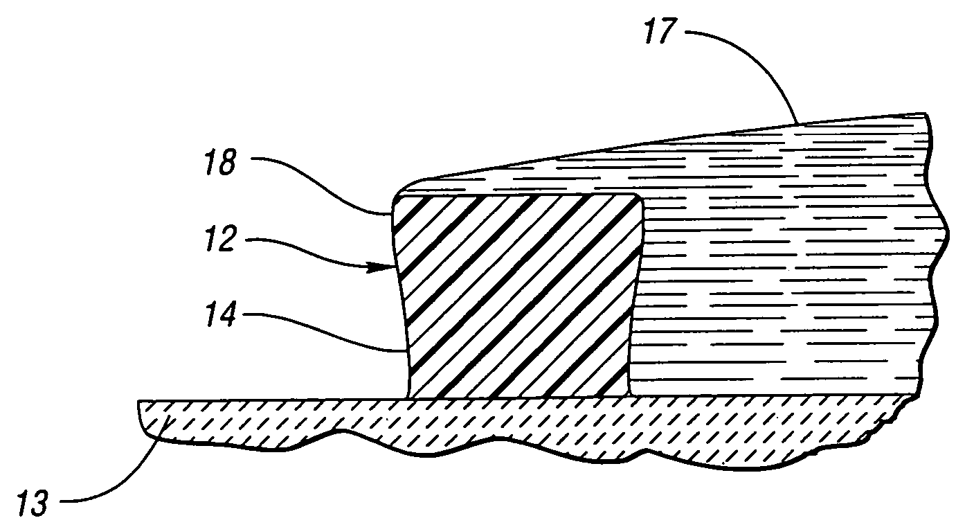
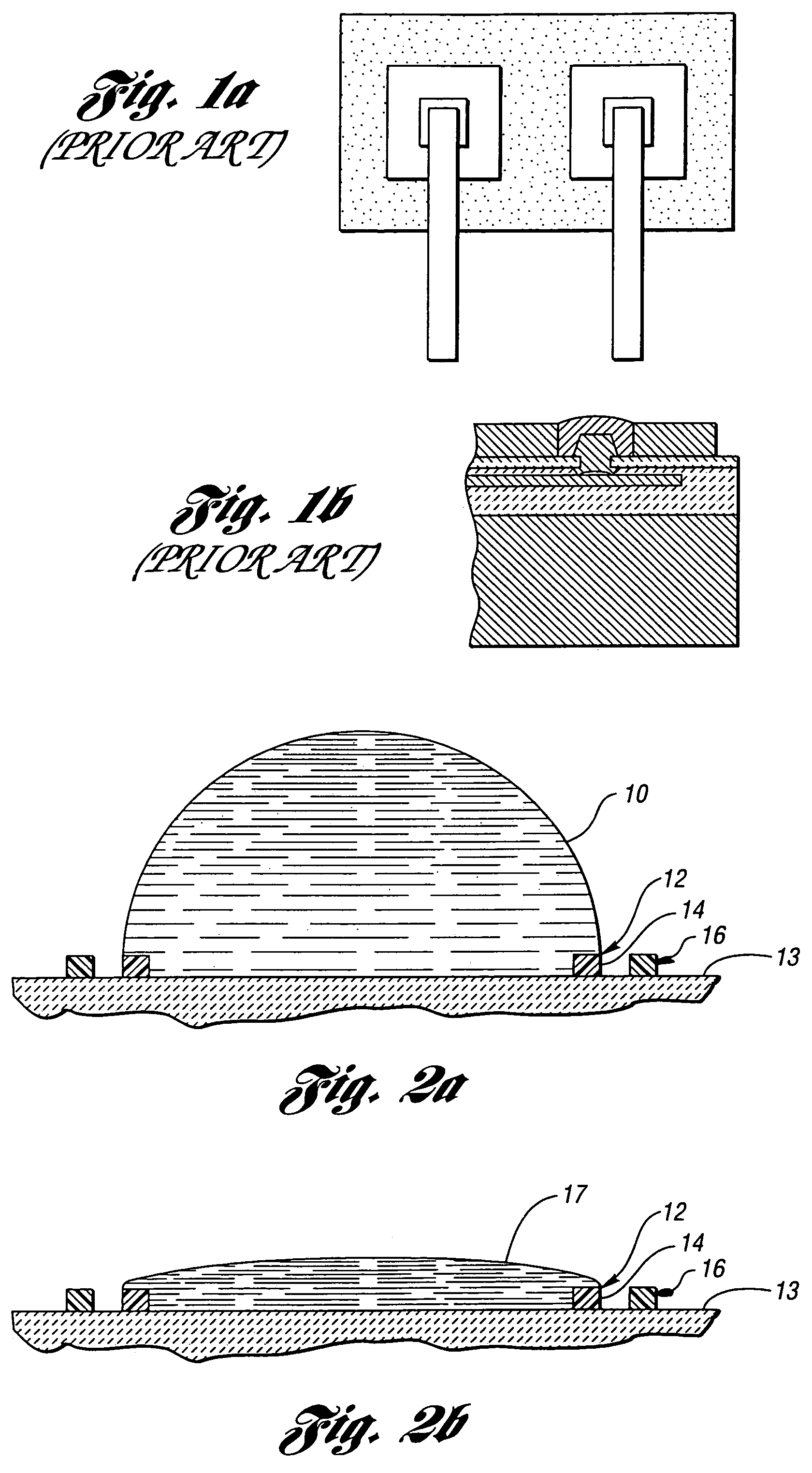
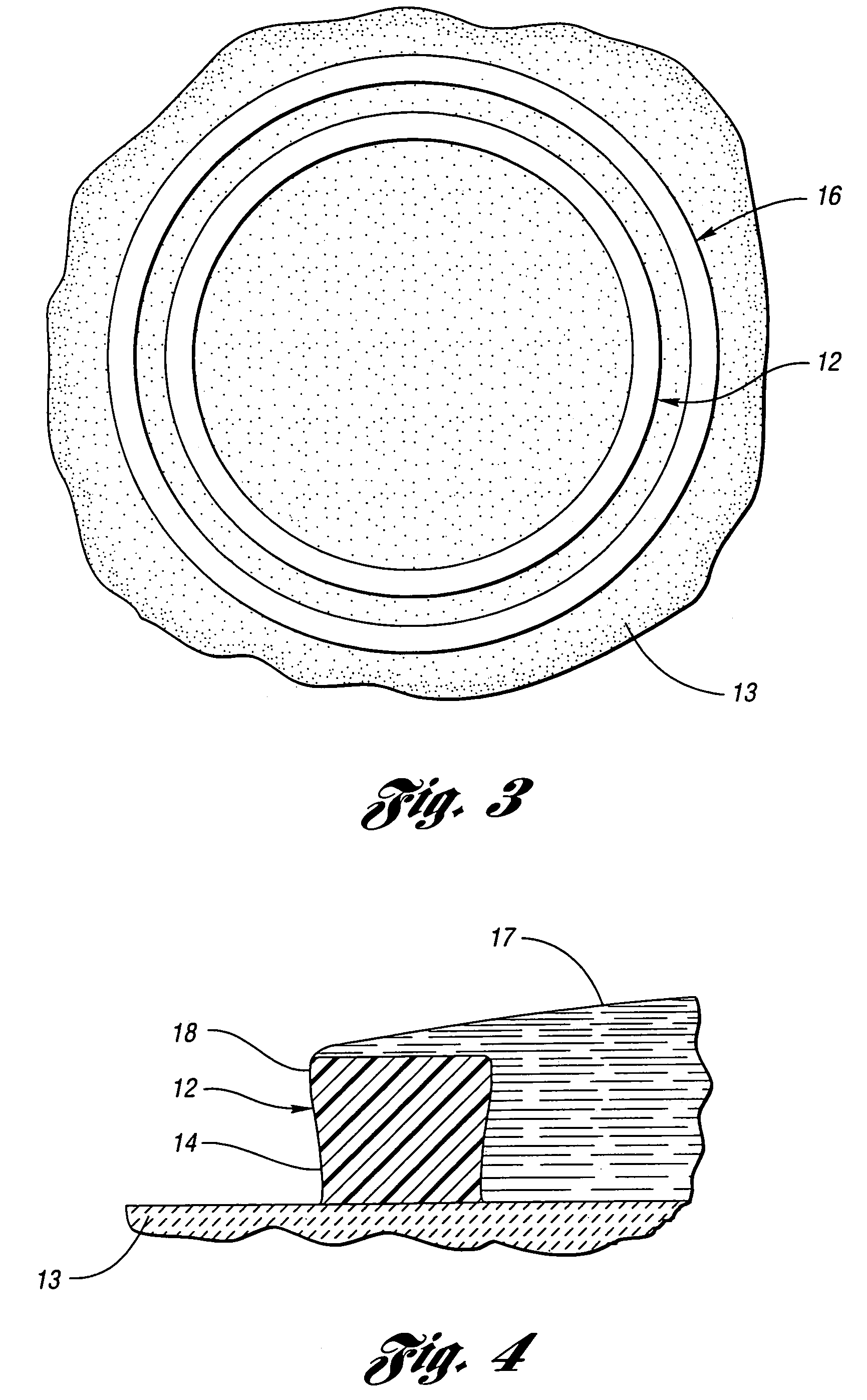
[0062]FIGS. 2a and 2b show the thin well approach for dispensed membranes of the present invention. To achieve membranes of the desired thickness, it is necessary to confine a large amount of membrane / solvent solution in a small area. When a membrane 10 is deposited, it covers the top of an inner well, generally indicated at 12, formed on an insulating layer 13 of a semiconductor substrate. Surface tension in the membrane solution 10 stops it from flowing past a vertical wall 14 at a rounded outside edge or corner 18 of the well 12, as best shown in FIG. 4.
[0...
PUM
| Property | Measurement | Unit |
|---|---|---|
| Thickness | aaaaa | aaaaa |
| Thickness | aaaaa | aaaaa |
| Thickness | aaaaa | aaaaa |
Abstract
Description
Claims
Application Information


