Semiconductor integrated circuit device

a technology of integrated circuit devices and semiconductors, applied in the direction of transistors, electrical devices, arrangements responsive to excess voltage, etc., can solve the problems of increasing the resistance of surges, and affecting the protection performance of the protected circuit 105/b>, so as to achieve high esd protection performance and increase the resistance to surges

Inactive Publication Date: 2008-10-21
PANASONIC CORP
View PDF15 Cites 26 Cited by
  • Summary
  • Abstract
  • Description
  • Claims
  • Application Information

AI Technical Summary

Benefits of technology

[0012]In order to achieve this object, a semiconductor integrated circuit device including an SCR protection circuit according to the present invention has a configuration in which an RC circuit is used for a trigger circuit for generating trigger current in the SCR protection circuit. This configuration allows control of a voltage at which trigger current for starting the SCR protection circuit is generated so that the ON voltage of the SCR protection circuit is lower than the breakdown value of the gate oxide film of a transistor in a protected circuit.
[0014]In this semiconductor integrated circuit device according to the present invention, as trigger current in the SCR protection circuit, not breakdown current of, for example, a MOS transistor but ON current of the MOS transistor is allowed to be used. Accordingly, the SCR protection circuit turns ON at a voltage lower than the breakdown voltage of the gate oxide film of a transistor forming a protected circuit. As a result, even if the process (design rule) is miniaturized, the resistance against surges is increased so that a high ESD protection performance ability satisfying a criterion of a surge withstand test is obtained.

Problems solved by technology

With recent developments of technology in processing field, such as miniaturization and increase in density, semiconductor integrated circuit devices are more and more susceptible to damage from ESD (hereinafter, referred to as a surge).
For example, there is an increasing possibility that a surge entering from an external connector pad destroys a device, such as an input circuit, an output circuit, an input / output circuit or an internal circuit, to cause degradation of device performance.
However, in the conventional semiconductor integrated circuit device, when a surge of positive charge is applied to the power line 101 with the ground line 102 grounded, the protected circuit 105 might be destroyed under miniaturization in processing.

Method used


Image

  • Semiconductor integrated circuit device
  • Semiconductor integrated circuit device
  • Semiconductor integrated circuit device

Examples


embodiment 1

[0041]A first embodiment of the present invention will be described with reference to the drawings.

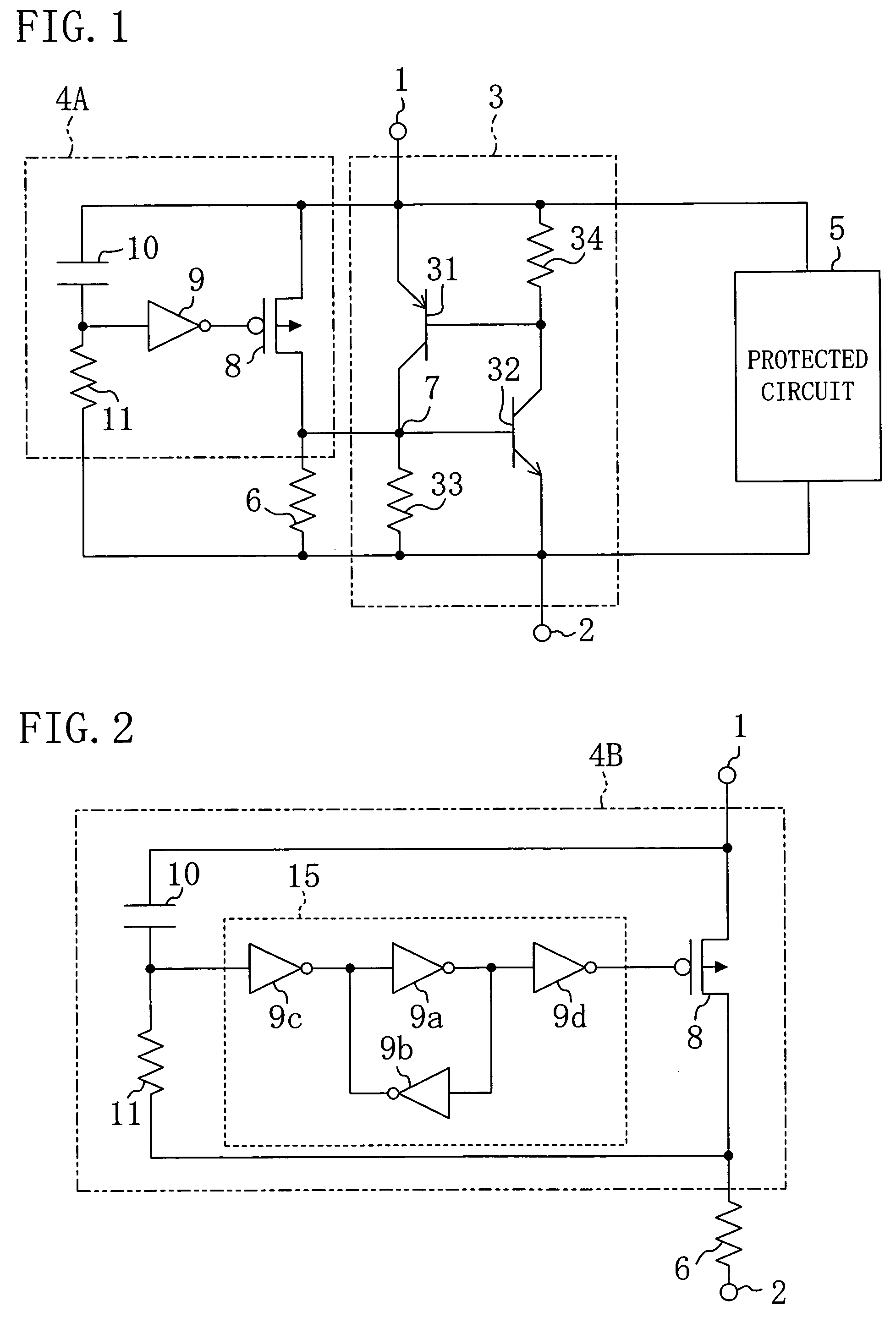
[0042]FIG. 1 illustrates a circuit configuration of a semiconductor integrated circuit device according to the first embodiment. As illustrated in FIG. 1, the semiconductor integrated circuit device of the first embodiment includes: an SCR protection circuit 3 provided between a power line 1 and a ground line 2; a trigger circuit 4A connected in parallel with the SCR protection circuit 3; and a protected circuit 5 protected by the SCR protection circuit 3 and including a MOS transistor (not shown).

[0043]The SCR protection circuit 3 includes: a pnp bipolar transistor 31 having its emitter connected to the power line 1 and the collector connected to a first trigger terminal 7; an npn bipolar transistor 32 having its emitter connected to the ground line 2, the collector connected to the base of the pnp bipolar transistor 31 and the base connected to the first trigger terminal 7; a first r...

modified example 1 of embodiment 1

[0051]FIG. 2 illustrates a trigger circuit in a semiconductor integrated circuit device according to a first modified example of the first embodiment. In FIG. 2, components already shown in FIG. 1 are denoted by the same numerals, and the description thereof will be omitted.

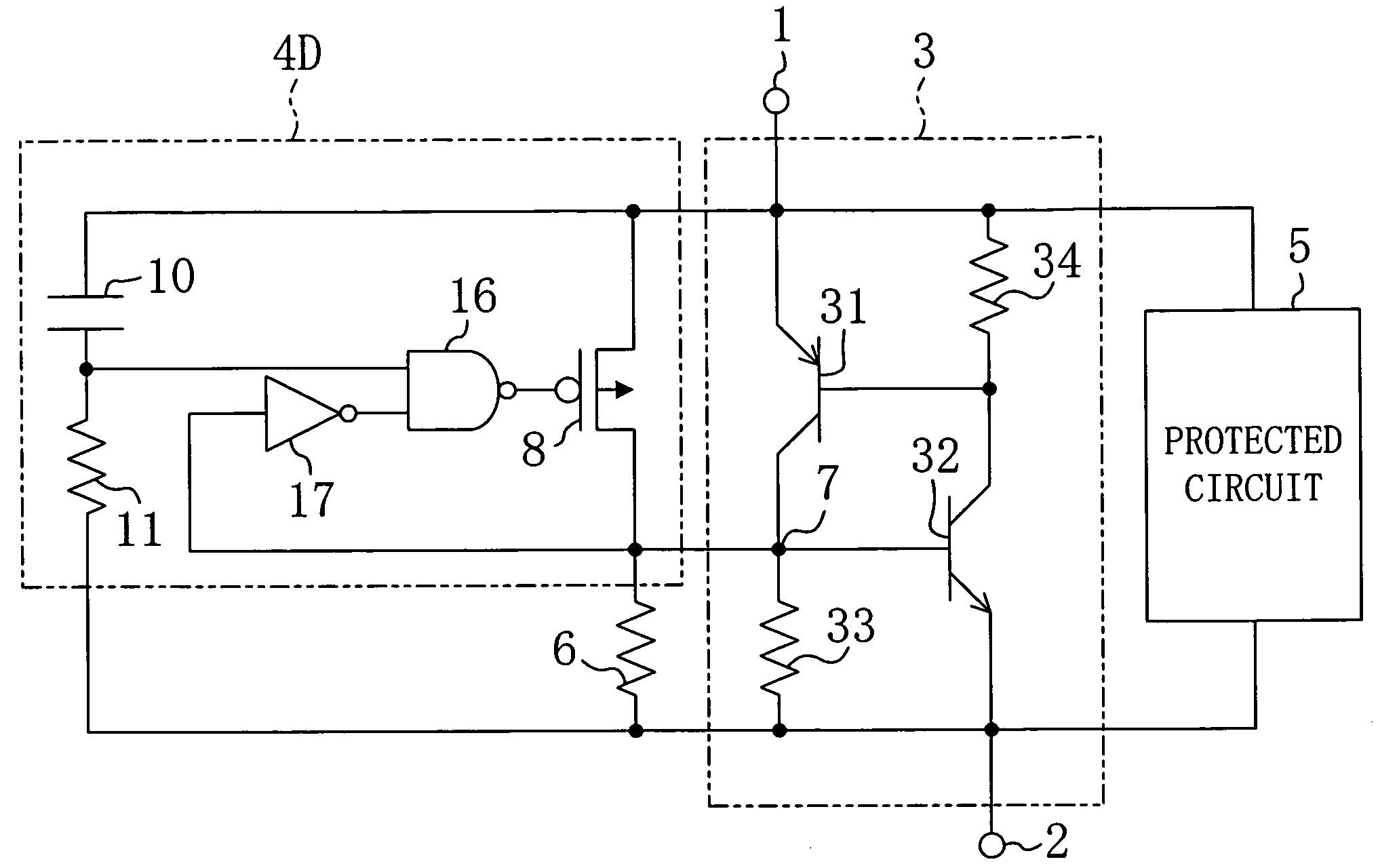
[0052]As illustrated in FIG. 2, a trigger circuit 4B according to this modified example includes a Schmitt trigger circuit 15 including, for example, a bistable circuit formed by two inverters 9a and 9b connected to form a flip-flop and inverters 9c and 9d connected to the input terminal and the output terminal, respectively, of the bistable circuit, instead of one inverter for applying a control voltage to the gate of the pMOS transistor 8.

[0053]In this manner, the Schmitt trigger circuit 15 prevents malfunction (latch-up) of the SCR protection circuit caused by power noise during normal operation.

modified example 2 of embodiment 1

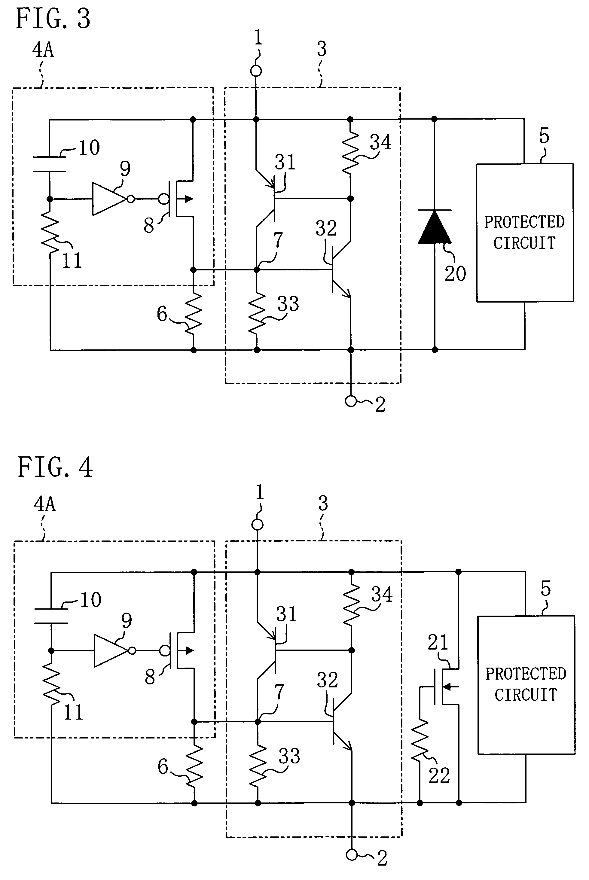
[0054]FIG. 3 illustrates a semiconductor integrated circuit device according to a second modified example of the first embodiment. In FIG. 3, components already shown in FIG. 1 are denoted by the same numerals, and the description thereof will be omitted.

[0055]As illustrated in FIG. 3, the semiconductor integrated circuit device of the second modified example includes a pn diode 20 connected in parallel with the protected circuit 5 and having its cathode connected to the power line 1 and the anode connected to the ground line 2.

[0056]With this configuration, even when a surge of positive charge is applied to the ground line 2 with the power line 1 grounded, a positive bias voltage is applied to the pn diode 20, so that the power line 1 and the ground line 2 become conductive. Accordingly, surge charge is discharged from the ground line 2 to the power line 1. As a result, even when a surge of positive charge is applied to the ground line 2, destruction of the gate oxide film of the M...


PUM


Abstract

A semiconductor integrated circuit device includes: a protected circuit protected against electro-static discharge applied from outside the device; an SCR protection circuit having an anode terminal connected to a power line, a cathode terminal connected to a ground line and a trigger terminal; and a trigger circuit connected to the trigger terminal and including an RC circuit connected between the power line and the ground line.

Description

CROSS-REFERENCE TO RELATED APPLICATION[0001]The disclosure of Japanese Patent Application No. 2005-77411 filed in Japan on Mar. 17, 2005 including specification, drawings and claims is incorporated herein by reference in its entirety;BACKGROUND OF THE INVENTION[0002]The present invention relates to semiconductor integrated circuit devices including electro-static discharge (ESD) protection circuits, and particularly relates to semiconductor integrated circuit devices including silicon-controlled rectifier (SCR) protection circuits incorporated in ESD protection circuits.[0003]With recent developments of technology in processing field, such as miniaturization and increase in density, semiconductor integrated circuit devices are more and more susceptible to damage from ESD (hereinafter, referred to as a surge). For example, there is an increasing possibility that a surge entering from an external connector pad destroys a device, such as an input circuit, an output circuit, an input / ou...

Claims


Application Information

Patent Timeline
Patent Type & Authority Patents(United States)
IPC IPC(8): H02H3/20H02H3/22H02H9/04
CPCH01L27/0262
Inventor ARAI, KATSUYAKOUGAMI, TOSHIHIROKAMEI, MASAYUKI
Owner PANASONIC CORP
Why Eureka
Try Eureka