Electromagnetic interference shielding for a printed circuit board

a technology of printed circuit board and electromagnetic interference, which is applied in the direction of localised screening, electrical apparatus construction details, and semiconductor/solid-state device details, etc., can solve the problems of increasing the cost of manufacturing electronic equipment such as cell phones, personal digital assistants, and high cost of existing solutions, so as to reduce the amount of electromagnetic interference

Active Publication Date: 2008-10-28
DEEP COAT +1
View PDF14 Cites 96 Cited by
  • Summary
  • Abstract
  • Description
  • Claims
  • Application Information

AI Technical Summary

Benefits of technology

[0016]The plurality of conductive vias may strategically be formed in a pattern through the printed circuit board so as to reduce the amount of electromagnetic interference that is able to pass through the printed circuit board. Preferably, the vias are spaced from each other no more than about ½ to about ¼ of a wavelength of a highest frequency or harmonic frequency of the electromagnetic interference of an electronic component on the printed circuit board. As such, depending on the electronic component, the vias may be spaced between about 1 mm and 200 mm from each other.
[0023]In one embodiment, the network of conductive elements comprise a plurality of conductively coated or filled vias. The spaces between adjacent vias comprise a largest dimension that is small enough to substantially reduce emission of electromagnetic radiation from the electronic component. Preferably, the largest dimension is no more than about ½ to about ¼ of a wavelength of a highest frequency or harmonic frequency of the electromagnetic interference of an electronic component on the printed circuit board. As such, depending on the electronic component, the vias may be spaced between about 1 mm and 200 mm from each other.

Problems solved by technology

The problem of emittance of electromagnetic radiation is not new to designers of electronic equipment.
In virtually all cases, the existing solutions are expensive and add to the cost of manufacturing electronic equipment such as cell phones, personal digital assistants, laptop computers, set-top boxes, cable modems, networking equipment including switches, bridges, and cross-connects.
Unfortunately, the material has proven to be expensive, difficult to use, and subject to inferior performance due to cracking of the aluminum fiber layer.
The Koskenmaki aluminum fiber metal layers had limitations on the ability to withstand a thermoforming process due to the typical tight radius used in the thermoforming molds.
However, as the frequency of chips increase (e.g., greater than 1 GHz) and the data transmission rates increase, the creation of errant EMI radiation becomes much easier and more harmful to circuits and components located nearby.
Thus, in general, conventional solutions will increasingly find themselves inadequate for purposes of immunity and indeed, radiated emissions, may also become an increasing issue.
Moreover, for microwave devices, especially those that operate of have harmonic frequencies above about 10 GHz., radiated emissions will be a significant concern.
In general, as can be seen in FIG. 1, there is nothing in the conventional shielding solution to contain the radiation escaping from the bottom of the chip 12 and through the PCB 10 except for the phenomena of partial reflection from the ground plane 20 (sometimes referred to herein as an “image” plane) which can, in some situation, improve the radiation emissions problem but is problematical from a design and manufacturing point to achieve.

Method used


Image

  • Electromagnetic interference shielding for a printed circuit board
  • Electromagnetic interference shielding for a printed circuit board
  • Electromagnetic interference shielding for a printed circuit board

Examples


Embodiment Construction

[0064]The present invention provides improved printed circuit boards, electronic devices, and EMI shielding, and methods of manufacturing the improved printed circuit boards, electronic devices, and EMI shielding.

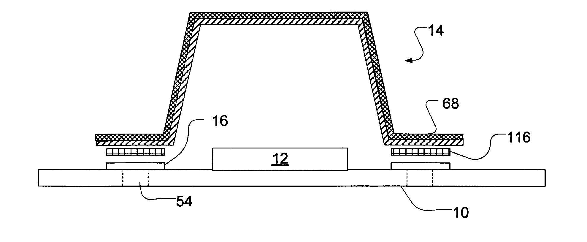
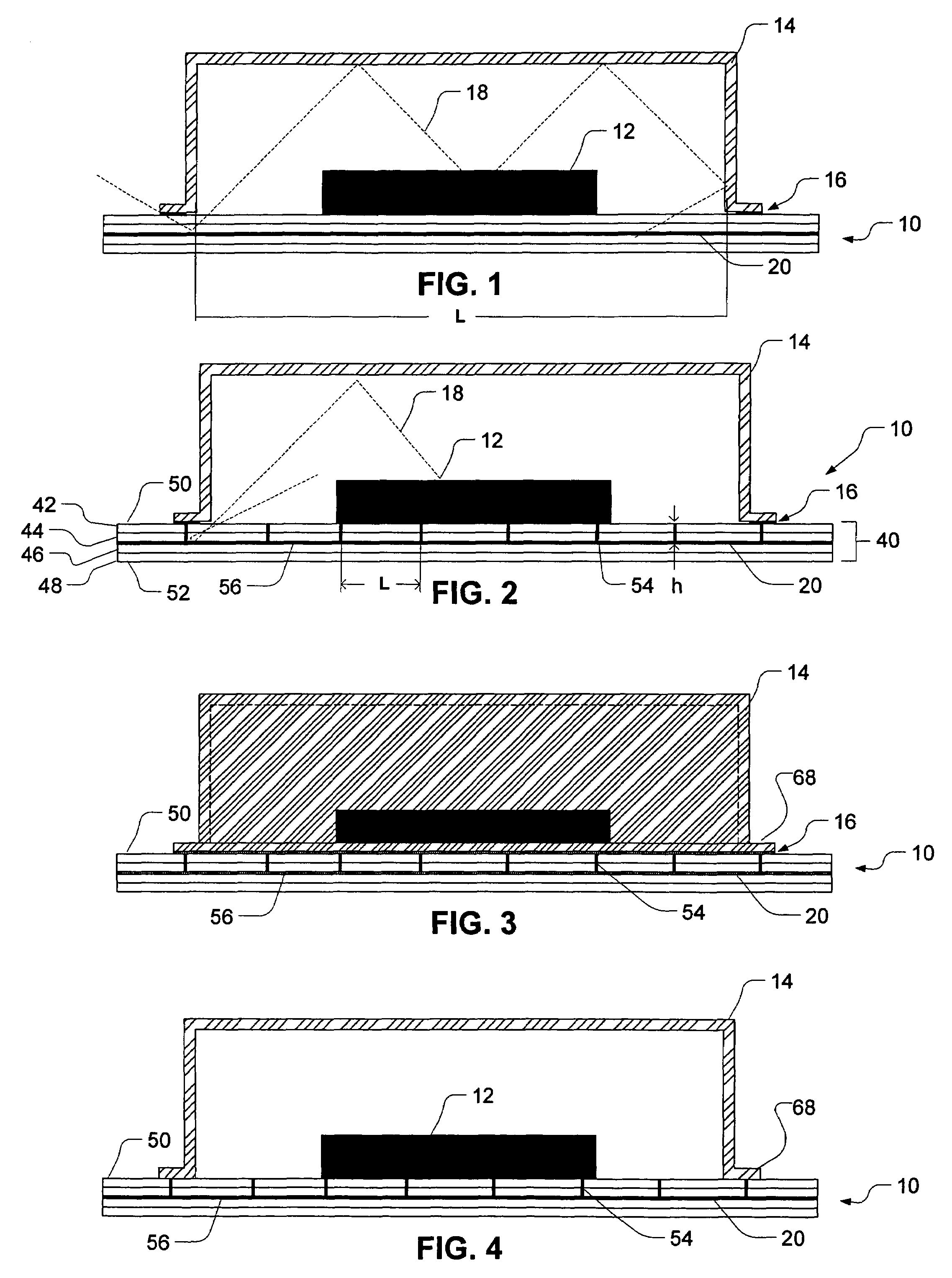
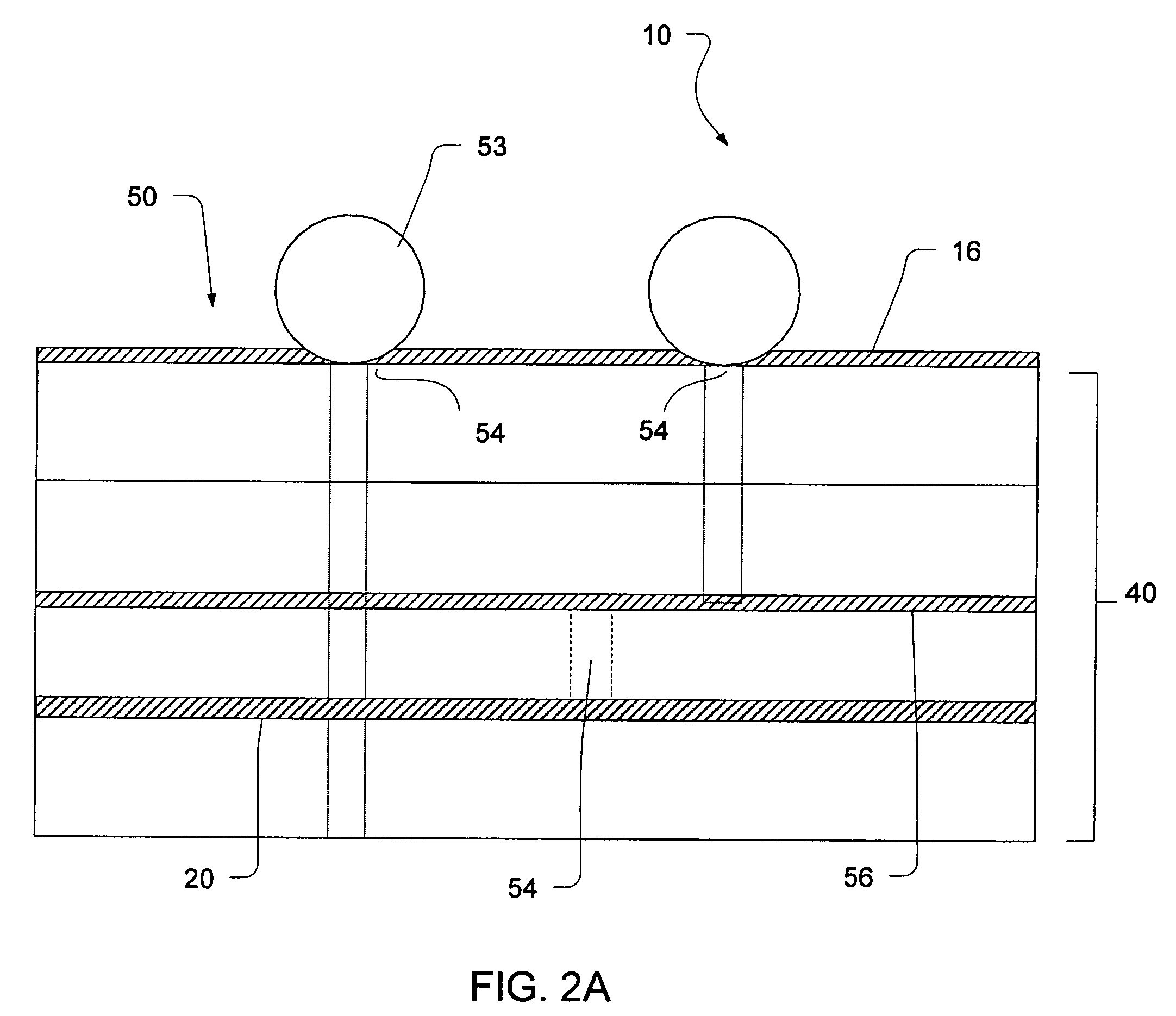
[0065]FIGS. 2 and 3 illustrate a printed circuit board printed circuit board 10 that is encompassed by the present invention. Printed circuit board 10 comprises conductive traces superimposed or printed on one or both surfaces (not shown) and may also contain internal signal layers (not shown), power planes (not shown) and one or more ground planes 20. Printed circuit board 10 comprises one or more layers of insulative organic or inorganic material containing the pattern(s) of conductive traces. Printed circuit board 10 becomes an electrical circuit when electronic components 12 are attached to one of the printed circuit board's surfaces and leads from the electronic component are contacted with the conductive traces.

[0066]While printed circuit board 10 may be composed of a...


PUM


Abstract

The present invention provides shielded printed circuit boards and electronic devices. The printed circuit board may comprise an internal network of grounded conductive elements that are coupleable to an EMI shield that is mounted on the printed circuit board. The network of grounded conductive elements are coupleable to a grounded layer and to the EMI shield and provides improved EMI shielding through the volume of the printed circuit board below an electronic component mounted on the printed circuit board.

Description

CROSS-REFERENCES TO RELATED APPLICATIONS[0001]The present application claims benefit to provisional U.S. Patent Application Ser. No. 60 / 462,902, filed Apr. 15, 2003, the complete disclosure of which is incorporated herein by reference.[0002]The present invention is also related to U.S. patent application Ser. No. 10 / 825,747, filed herewith, and entitled “EMI Shielding for Electronic Component Packaging,” the complete disclosure of which is incorporated herein by referenceBACKGROUND OF THE INVENTION[0003]The present invention generally relates to shielded electronic devices and printed circuit boards. More specifically, the present invention provides an EMI shield coupled to a surface of the printed circuit board and an EMI shield that is formed within the printed circuit board.[0004]Electronic products emit electromagnetic radiation, generally in the range of 50 MHz to 3 GHz, but not limited to this range, especially in light of the many advances in high-speed microprocessor design ...

Claims


Application Information

Patent Timeline
Patent Type & Authority Patents(United States)
IPC IPC(8): H05K7/14H05K7/18H01L23/04H01L23/31H01L23/433H01L23/485H01L23/49H01L23/498H01L23/50H01L23/552H05K1/02H05K3/34
CPCH01L23/04H01L23/3128H01L23/315H01L23/4334H01L23/49816H01L23/49822H01L23/49838H01L23/50H01L23/552H01L24/49H05K1/0218H05K3/3484H01L21/50H01L24/16H01L24/48H01L2224/16H01L2224/48091H01L2224/48227H01L2224/49171H01L2224/49175H01L2224/73253H01L2924/01006H01L2924/01013H01L2924/01014H01L2924/01027H01L2924/01028H01L2924/01029H01L2924/01033H01L2924/01047H01L2924/0105H01L2924/01074H01L2924/01078H01L2924/01079H01L2924/01082H01L2924/14H01L2924/15192H01L2924/15311H01L2924/1532H01L2924/16152H01L2924/1617H01L2924/16315H01L2924/166H01L2924/3011H01L2924/3025H05K2201/10734H01L2924/014H01L2224/48233H01L2224/32225H01L2224/73265H01L2924/07802H01L2224/16235H01L2924/00014H01L2924/00H01L2924/181H05K9/003H01L2924/12042H05K9/0035H01L2224/45099H01L2224/05599
Inventor ARNOLD, ROCKY R.ZARGANIS, JOHN C.MONTAUTI, FABRIZIO
Owner DEEP COAT
Why Eureka
Try Eureka