Method for the growth of large low-defect single crystals

a single crystal, widebandgap technology, applied in the direction of single crystal growth, polycrystalline material growth, condensed vapor growth, etc., can solve the problems of high dislocation density of the resulting wafer, high cost, and high cost, so as to reduce unwanted deposition and reduce cost , greatly enhance performance and reliability

Inactive Publication Date: 2008-11-11
NASA +1
View PDF13 Cites 41 Cited by
  • Summary
  • Abstract
  • Description
  • Claims
  • Application Information

AI Technical Summary

Benefits of technology

[0063]This process is particularly suitable for wide-bandgap semiconductors, such as SiC, III-Nitride compounds and their alloys, and diamond. In another embodiment of the current invention applied to the growth of bulk crystals with a wurtzite, zincblende, or diamond cubic structure, epitaxial axial growth can take place in the first growth region without the presence of any screw dislocations for the growth of the small seed crystal. Also, in other preferred embodiments (irrespective of the crystal structure and material), epitaxial axial growth of the tip portion of the LTC seed can take place in the first growth region by either (1) a vapor-solid (VS) process, (2) a vapor-liquid-solid (VLS) process, or (3) a combination of the traveling solvent method (TSM) and the laser heated pedestal growth (LHPG) method. In other embodiments, crystal heating methods for growth at the tip portion in region 1 include focused optical (e.g. laser) heating and shaped radiant heaters. Also, preferred temperature gradients and preferred flow patterns in the first growth region can be used to promote approximate columnar (with axis parallel to the growth direction) growth morphology in the first growth region. Additional preferred embodiments include various processes for the second growth region. These include hot-wall Chemical Vapor Deposition (CVD) using an inductively heater susceptor, or warm-wall CVD using direct inductive heating of the LTC seed. Various purge gas flows can be used to reduce unwanted deposition on surfaces other than intended crystal surfaces. Other embodiments of the invention include (1) continuous growth with removal of the completed boule accomplished in situ during the growth process, (2) with the process interrupted, removal of the completed boule in situ after interrupting the growth and cooling to some suitable temperature, (3) significant physical separation between the first and second growth regions, and (4) axial growth of the columnar portion of the LTC seed with an extended length in a first growth reactor, and lateral growth on the columnar portion of the LTC seed with an extended length at some later time in a suitable second growth reactor. In all of the embodiments described, the presence of the third region (of no growth) is optional. Mass production of large low-defect single crystals of WBG semiconductors at lower cost, that this invention enables, will in turn enable greatly enhanced performance and reliability for applications involving high power, high voltage, high frequency, and / or high temperature operating conditions.

Problems solved by technology

With prior art, growth is predominantly in the c-axis direction with detrimentally multiple screw dislocations providing the steps for step-flow growth and detrimentally higher growth temperatures, resulting in wafers with high dislocation densities throughout the resulting wafer area.
This prior art requires multiple screw dislocations in order to achieve high growth rates and multiple screw dislocations disadvantageously lead to problems of coalescence of steps from multiple step sources.
With prior art, much waste is incurred because of the varying diameter and non-symmetrical shape of the boule.
With prior art, controlling and modifying the temperature profile at the growth front during growth becomes increasingly difficult as the diameter increases.

Method used


Image

  • Method for the growth of large low-defect single crystals
  • Method for the growth of large low-defect single crystals
  • Method for the growth of large low-defect single crystals

Examples


Embodiment Construction

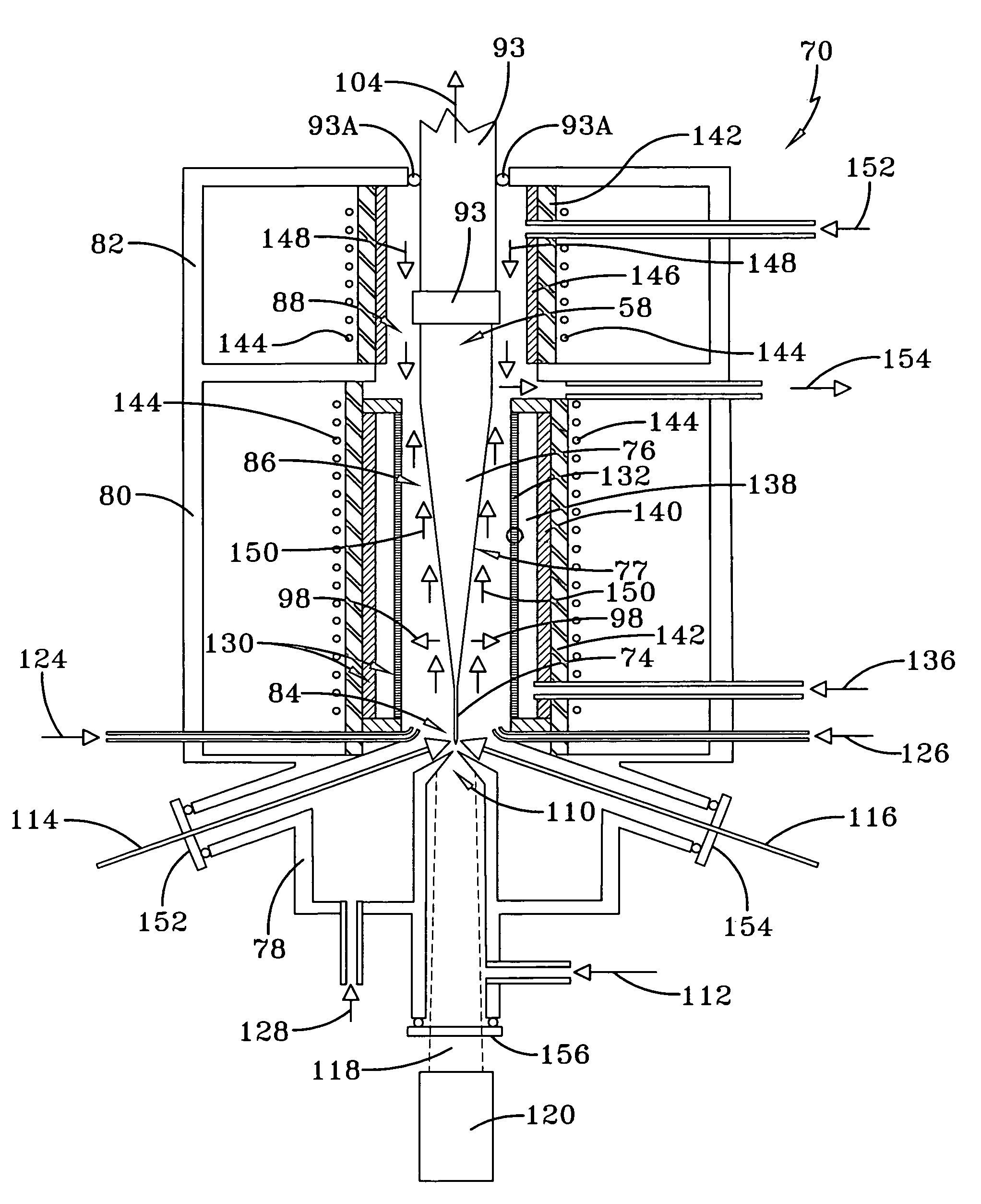
[0082]In general, the present invention provides methods, growth reactors, and the beneficial products resulting therefrom for the crystal growth of large, low-defect tetrahedrally-bonded single crystals. The inventive process utilizes a large tapered crystal seed, herein referred to as an LTC seed, that has a defined central axis parallel to a preferred crystal direction, a base having a center and opposite upper and lower portions and with the base's upper portion attached to a holder, a tapered portion that extends downward along the central axis from the lowermost portion of the base, a columnar portion having a center and that extends downward from the lowermost portion of the tapered portion along the central axis of the LTC seed, with a defined diameter of the columnar portion smaller than a defined diameter of the base, and with lowermost end of the columnar portion defined to be the tip portion of the LTC seed, and with the central axis of the LTC seed defined to pass throu...


PUM


Abstract

A method and the benefits resulting from the product thereof are disclosed for the growth of large, low-defect single-crystals of tetrahedrally-bonded crystal materials. The process utilizes a uniquely designed crystal shape whereby the direction of rapid growth is parallel to a preferred crystal direction. By establishing several regions of growth, a large single crystal that is largely defect-free can be grown at high growth rates. This process is particularly suitable for producing products for wide-bandgap semiconductors, such as SiC, GaN, AlN, and diamond. Large low-defect single crystals of these semiconductors enable greatly enhanced performance and reliability for applications involving high power, high voltage, and/or high temperature operating conditions.

Description

ORIGIN OF THE INVENTION[0001]The invention described herein was made in the performance of work under NASA contracts and is subject to the provisions of Section 305 of the National Aeronautics and Space Act of 1958, Public Law 85-568 (72 Stat. 435; 42 U.S.C. 2457).FIELD OF THE INVENTION[0002]The invention relates to the crystal growth of wide-bandgap semiconductor bulk crystals, and more particularly, to a method for growing relatively large single crystals that are nearly free of extended structural crystal defects. In some embodiments, the invention provides a method that utilizes single-dislocation-assisted growth of the small-diameter end of a large tapered crystal seed in an axial direction parallel to a selected crystal direction, combined with lateral growth on the side wall of the large tapered crystal seed. In other embodiments, crystal growth proceeds without dislocations. The invention has application in the growth of single crystals to be used as (a) semiconducting mater...

Claims


Application Information

Patent Timeline
Patent Type & Authority Patents(United States)
IPC IPC(8): C30B25/12C30B25/14
CPCC30B11/14C30B23/025C30B25/18C30B29/36
Inventor POWELL, J. ANTHONYNEUDECK, PHILIP G.TRUNEK, ANDREW J.SPRY, DAVID J.
Owner NASA
Why Eureka
Try Eureka