Nitride-based semiconductor device
a technology of nitride and semiconductors, applied in the direction of semiconductor devices, basic electric elements, electrical equipment, etc., can solve the problems of difficult nitride-based semiconductors
- Summary
- Abstract
- Description
- Claims
- Application Information
AI Technical Summary
Benefits of technology
Problems solved by technology
Method used
Image
Examples
first embodiment
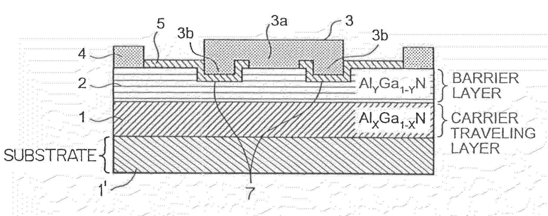
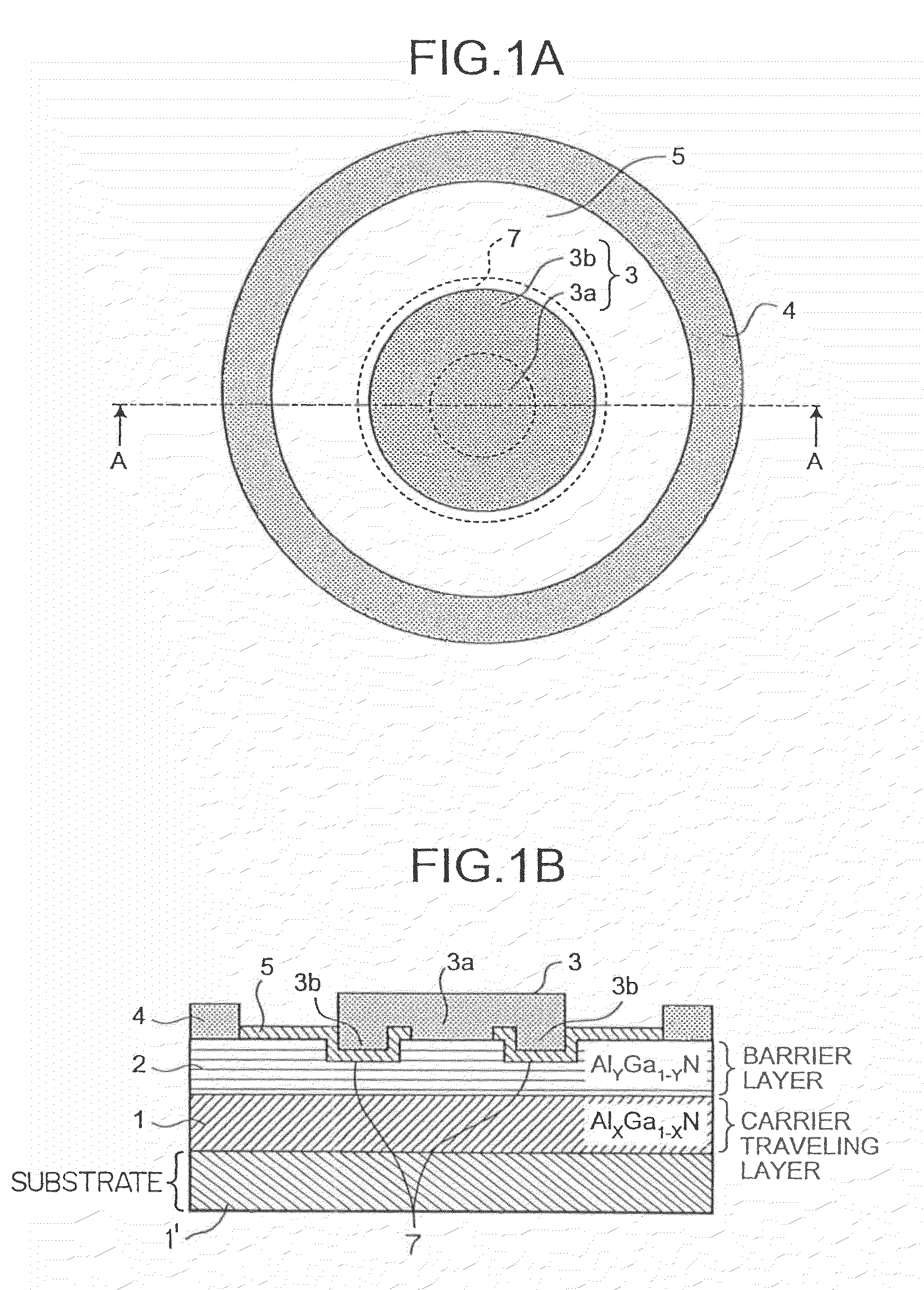
[0036]FIG. 1A is a schematic plan view of a nitride-based semiconductor device and FIG. 1B is a cross-section taken along the line A-A of FIG. 1A. The nitride-based semiconductor device is obtained by successively laminating a carrier traveling layer 1 and a barrier layer 2 on a substrate 1′, and forming an anode electrode 3 on the barrier layer 2 and also a cathode electrode 4 thereon so as to surround the anode electrode 3. Specifically, the carrier traveling layer 1 is made of AlXGa1-XN (0≦X2 is made of AlYGa1-YN (01.
[0037]The example of FIG. 1A shows that the planar shape of the anode electrode 3 is a circle, and that the planar shape of the cathode electrode 4 is a circular ring shape formed at a position apart from a peripheral portion 3b of the anode electrode 3 by a predetermined distance so as to surround the anode electrode 3. However, any shape may be used if the cathode electrode 4 surrounds the anode electrode 3. It is noted that the carrier traveling layer 1 correspon...
second embodiment
[0064]FIG. 12 is a schematic cross-sectional view of a nitride-based semiconductor device according to a The planar structure of the nitride-based semiconductor device is assumed, as shown in FIG. 10, that the anode electrode 3 is surrounded by the recess structure 7 and the element separating region 8. In the nitride-based semiconductor device shown in FIG. 12, an insulating film 9 is formed over the whole surface of the nitride-based semiconductor device having the cross-sectional structure shown in FIG. 1B, and a field plate electrode 10 is formed on the insulating film 9. The cross-section of the field plate electrode 10 is such that its edge is located in between the edge of the anode electrode 3 and the edge of the cathode electrode 4 on its anode electrode 3 side.
[0065]When the anode electrode 3 of the nitride-based semiconductor device is applied with reverse bias to be turned to the off-state, the electric field concentration occurring near the anode electrode 3 is relieve...
third embodiment
[0072]The method of manufacturing the nitride-based semiconductor device, in which the diode 11 and the field effect transistor 12 shown in FIG. 13A and FIG. 13B are formed on the same substrate, is explained below. FIG. 14A to FIG. 14I are schematic cross-sectional views of one example of a procedure for the method of manufacturing the nitride-based semiconductor device according to the At first, as shown in FIG. 14A, the carrier traveling layer 1 and the barrier layer 2 are successively grown in the diode forming region RD and the transistor forming region RTR on a substrate (not shown) on which a predetermined film is formed if necessary. Specifically, the carrier traveling layer 1 is made of a non-doped AlXGa1-XN (0≦X2 is made of a non-doped or n-type AlYGa1-YN (01 and the barrier layer 2 are formed by using the epitaxial crystal growth technique such as the MOCVD method that can control the film thickness at a level of atomic layer. The film thickness of the barrier layer 2 ne...
PUM
 Abstract
Description
Claims
Application Information


