Inverted mounting LED chip based on double-faced shrinkage pool substrate and component gradual change buffer layer

A LED chip and component gradient technology, applied in semiconductor devices, electrical components, circuits, etc., can solve problems such as unsatisfactory interface characteristics, lattice mismatch between sapphire substrate and GaN emission layer, etc., and increase the range of growth stress , fewer dislocation defects, and improved light extraction efficiency

Inactive Publication Date: 2011-08-17
CHONGQING UNIV
View PDF5 Cites 35 Cited by
  • Summary
  • Abstract
  • Description
  • Claims
  • Application Information

AI Technical Summary

Problems solved by technology

[0005] Aiming at the current situation that the existing sapphire substrate does not match the GaN emission layer lattice and the interface properties are not ideal, the present invention provides a flip-chip LED chip based on a double-sided concave hole substrate and a composition gradient buffer layer

Method used


Image

  • Inverted mounting LED chip based on double-faced shrinkage pool substrate and component gradual change buffer layer
  • Inverted mounting LED chip based on double-faced shrinkage pool substrate and component gradual change buffer layer
  • Inverted mounting LED chip based on double-faced shrinkage pool substrate and component gradual change buffer layer

Examples


Embodiment Construction

[0022] The present invention will be described in further detail below in conjunction with the accompanying drawings and specific embodiments.

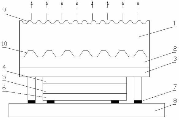
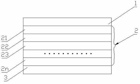
[0023] figure 1 It is a schematic structural diagram of a flip-chip LED chip based on a double-sided concave hole substrate and a composition-graded buffer layer, figure 2 for Al x Ga 1-x The schematic diagram of the structure of the N-component graded buffer layer is shown in the figure. An LED chip based on a double-sided concave hole substrate and a composition-graded buffer layer, the LED chip is composed of a sapphire substrate 1, an Al x Ga 1-x N composition graded buffer layer 2, n-type GaN epitaxial layer 3, InGaN / GaN multiple quantum well 4, p-type GaN layer 5, transparent ITO conductive film 6, flip-chip welding electrode 7 and silicon substrate 8 with good conductivity . The upper surface of the sapphire substrate 1 is uniformly provided with m concave holes I9, wherein m satisfies: 10 2 ≤m≤10 4 , the lower surfac...


PUM


Abstract

The invention discloses an inverted mounting LED chip based on double-faced shrinkage pool substrate and component gradual change buffer layer, wherein the chip comprises a sapphire substrate distributed with 102-104 shrinkage pools at upper and lower surfaces, an AlxGa1-xN component gradual change buffer layer composed of an unit layer formed by k non-doping AlxGa1-xN epitaxial materials, a n-type GaN epitaxial layer, an InGaN / GaN multi-quantum well, a p-type GaN layer, a transparent ITO (indium tin oxide) conductive film, an inverted mounting welding electrode and a silicon substrate from upper to lower. The LED chip disclosed by the invention uses the shrinkage pool structure for improving the emergent probability of LED emergent lights, and increasing the heat radiation area and growth stress acting range of the substrate, so that the GaB epitaxial quality and the radiation composite luminous efficiency are improved; the buffer layer of the n-type GaN epitaxial layer is manufactured by the AlxGa1-xN with gradually reduced Al component, so that the light-emitting efficiency and the internal quantum efficiency of the LED are improved, and a relatively high light output power is obtained.

Description

technical field [0001] The invention relates to the technical field of light-emitting diode chips, in particular to a chip based on substrate patterning, Al 1-x Ga x N ternary compound Al / Ga composition control technology and Ш-V group compound material epitaxy technology combined flip-chip LED chip based on double-sided concave hole substrate and composition gradient buffer layer. Background technique [0002] In recent years, with the improvement of GaN material preparation technology and p-type doping technology, GaN-based light-emitting diodes (LEDs) have been vigorously developed. At present, high-quality GaN-based epitaxial materials are mainly grown on insulating sapphire substrates through metal-organic chemical vapor deposition (MOCVD) technology. Since sapphire is not conductive, it is not possible to make LED electrodes on its surface. Using flip-chip welding technology, the LED chip with sapphire as the substrate is transferred to the substrate material with b...

Claims


Application Information

Patent Timeline
Patent Type & Authority Applications(China)
IPC IPC(8): H01L33/20H01L33/12
Inventor 杜晓晴钟广明陈伟民刘显明
Owner CHONGQING UNIV
Why Eureka
Try Eureka