Method of manufacturing a semiconductor device

a manufacturing method and semiconductor technology, applied in the direction of semiconductor devices, electrical devices, transistors, etc., can solve the problems of lowering the reliability of the semiconductor device, the dielectric breakdown resistance of the gate insulating film, etc., to improve the reliability, improve the electrical properties, and improve the performance

Active Publication Date: 2007-08-14
RENESAS ELECTRONICS CORP +1
View PDF5 Cites 32 Cited by
  • Summary
  • Abstract
  • Description
  • Claims
  • Application Information

AI Technical Summary

Benefits of technology

[0007]When a gate electrode formed by patterning a polycrystalline silicon film and a tungsten silicide film that are stacked over a gate insulating film disposed over a semiconductor substrate is subjected to heat treatment (light oxidation) in an oxygen atmosphere, oxidation of tungsten in the tungsten silicide film is likely to occur on the sidewalls of the gate electrode. This oxidation of tungsten on the sidewalls of the gate electrode may lower the dielectric breakdown resistance of the gate insulating film and, in turn, lower the reliability of the semiconductor device.
[0008]An object of the present invention is to provide a method of manufacture of a semiconductor device having improved reliability.
[0015]A semiconductor device having an improved performance can be obtained.
[0016]A semiconductor device having more improved electrical properties and improved reliability can be obtained.
[0017]A semiconductor device can be produced at an improved yield.

Problems solved by technology

This oxidation of tungsten on the sidewalls of the gate electrode may lower the dielectric breakdown resistance of the gate insulating film and, in turn, lower the reliability of the semiconductor device.

Method used


Image

  • Method of manufacturing a semiconductor device
  • Method of manufacturing a semiconductor device
  • Method of manufacturing a semiconductor device

Examples


embodiment 1

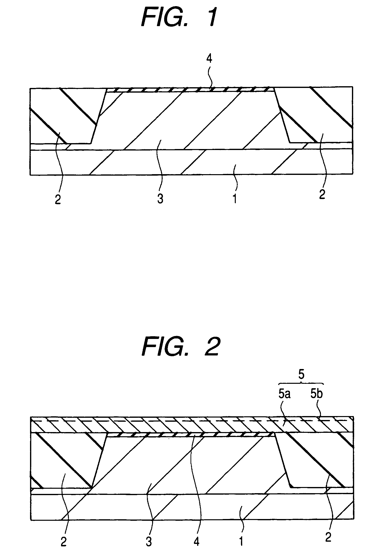
[0060]A method of manufacture of a semiconductor device according to this Embodiment will be described with reference to the drawings. FIGS. 1 and 2 are fragmentary cross-sectional views of a semiconductor device according to one embodiment of the present invention, for example, a MISFET (Metal Insulator Semiconductor Field Effect Transistor), during its manufacture.

[0061]As illustrated in FIG. 1, an element isolation region 2 is formed over the main surface of a semiconductor substrate (semiconductor wafer) 1 made of p type single crystal silicon having a specific resistance of about 1 to 10 Ωcm. The element isolation region 2 is made of silicon oxide and is formed, for example, by the STI (Shallow Trench Isolation) or LOCOS (Local Oxidization of Silicon) method. In this Embodiment, the STI method is employed for the formation of the element isolation region. In other words, the element isolation region 2 is formed by embedding a silicon oxide film in a trench formed in the semicon...

embodiment 2

[0099]FIG. 15 is a fragmentary cross-sectional view of a semiconductor device according to another embodiment of the present invention during its manufacturing step. In this Embodiment, the manufacturing steps as illustrated in FIG. 1 in Embodiment 1 can be similarly employed, and so a description thereof is omitted, and steps subsequent to those as illustrated in FIG. 1 will be described next.

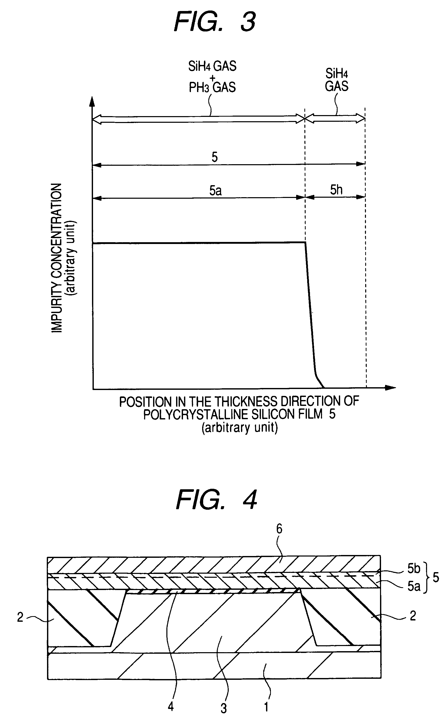
[0100]After the formation of the structure as illustrated in FIG. 1, a polycrystalline silicon film 5c is formed over the semiconductor substrate 1, more specifically, the gate insulating film 4 as illustrated in FIG. 15. The polycrystalline silicon film 5c is composed of polycrystalline silicon (doped polycrystalline silicon) doped with an impurity (for example, phosphorus (P)). The polycrystalline silicon film 5c can be formed, for example, by CVD and it can be formed by introducing monosilane (SiH4) and phosphine (PH3) gases into a film forming chamber of a film forming apparatus. A polycry...

embodiment 3

[0111]FIG. 20 is a fragmentary cross-sectional view of a semiconductor device according to a further embodiment of the present invention during its manufacturing step. In this Embodiment, the manufacturing steps as illustrated in FIG. 1 in Embodiment 1 can be similarly employed, and so a description thereof is omitted, and steps subsequent to those as illustrated in FIG. 1 will be described next.

[0112]After the formation of the structure as illustrated in FIG. 1, a polycrystalline silicon film 5e is formed over the semiconductor substrate 1, more specifically, the gate insulating film 4. The polycrystalline silicon film 5e can be formed, for example, by CVD.

[0113]FIG. 21 is a graph showing an impurity concentration distribution of the polycrystalline silicon film 5e in its thickness direction (a direction vertical to the main surface of the semiconductor substrate 1) after formation (deposition) and it corresponds to FIG. 3 of Embodiment 1. In FIG. 21, the abscissa corresponds to th...


PUM

PropertyMeasurementUnit
thicknessaaaaaaaaaa
temperatureaaaaaaaaaa
breakdown voltageaaaaaaaaaa

Abstract

For improving the reliability of a semiconductor device having a stacked structure of a polycrystalline silicon film and a tungsten silicide film, the device is manufactured by forming a polycrystalline silicon film, a tungsten silicide film and an insulating film successively over a gate insulating film disposed over the main surface of a semiconductor substrate, and patterning them to form a gate electrode having a stacked structure consisting of the polycrystalline silicon film and tungsten silicide film. The polycrystalline silicon film has two regions, one region formed by an impurity-doped polycrystalline silicon and the other one formed by non-doped polycrystalline silicon. The tungsten silicide film is deposited so that the resistivity of it upon film formation would exceed 1000 μΩcm.

Description

CROSS-REFERENCE TO RELATED APPLICATION[0001]The present application claims priority from Japanese Patent application JP 2003-299793, filed on Aug. 25, 2003, the content of which is hereby incorporated by reference into this application.BACKGROUND OF THE INVENTION[0002]The present invention relates to a technique for use in the manufacture of a semiconductor device; and, more particularly, the invention relates to a technique that is effective when applied to the manufacture of a semiconductor device which is equipped with a MISFET (Metal Insulator Semiconductor Field Effect Transistor) having a gate electrode obtained by stacking a polycrystalline silicon film and a tungsten silicide film one after another.[0003]A gate electrode having a stacked structure consisting of a polycrystalline silicon film and a tungsten silicide film is formed by forming a gate insulating film over a semiconductor substrate, forming thereover a polycrystalline silicon film and a tungsten silicide film suc...

Claims


Application Information

Patent Timeline
Patent Type & Authority Patents(United States)
IPC IPC(8): H01L21/44H01L21/336H01L21/4763H01L21/28H01L21/285H01L21/3205H01L21/768H01L21/8234H01L21/8238H01L21/8242H01L21/8247H01L27/088H01L27/092H01L27/10H01L27/105H01L27/108H01L27/115H01L29/423H01L29/49H01L29/78H01L29/788H01L29/792
CPCH01L21/28035H01L21/28525H01L21/32053H01L21/76886H01L21/82345H01L21/823462H01L21/823842H01L21/823857H01L27/105H01L27/115H01L27/11526H01L27/11546H01L29/4916H01L29/6659H01L29/7833H10B41/40H10B41/49H10B69/00
Inventor YAMADA, KENTAROTAKAHASHIKONAGAYA, TATSUYUKIKATOH, TAKESHISAKASHITA, MASAKITAKEI, KOICHIROOBARA, YASUHIROFUKAYAMA, YOSHIO
Owner RENESAS ELECTRONICS CORP
Why Eureka
Try Eureka