Method of fabricating thin film transistor

a thin film transistor and fabrication method technology, applied in the direction of gel state, crystal growth process, polycrystalline material growth, etc., can solve the problems of low electron mobility of cvd method, easy deformation of substrate, and damage to silicon layer by contained hydrogen cracking

Inactive Publication Date: 2008-11-18
SAMSUNG DISPLAY CO LTD
View PDF23 Cites 9 Cited by
  • Summary
  • Abstract
  • Description
  • Claims
  • Application Information

AI Technical Summary

Benefits of technology

[0009]The present invention, therefore, solves aforementioned problems associated with conventional devices by providing a method of fabricating a thin film transistor in which, in order to control the concentration of metal catalysts remaining on a polycrystalline silicon layer when an amorphous silicon layer formed on an insulating substrate is crystallized into the polycrystalline silicon layer using a super grain silicon (SGS) crystallization method, the substrate is annealed so that a very small amount of metal catalyst is adsorbed or diffused into a capping layer, and then a crystallization process is carried out, thereby minimizing the concentration of the metal catalysts remaining on the polycrystalline silicon layer, as well as forming a thick metal catalyst layer.

Problems solved by technology

However, the silicon layer directly deposited on the substrate by, for example, the CVD method has low electron mobility because it contains hydrogen of about 12%.
In addition, when the amorphous silicon layer having such low electron mobility is annealed and crystallized into a silicon layer of a crystalline structure having high electron mobility, the silicon layer is damaged by the cracking of the contained hydrogen.
However, the solid phase crystallization method has a disadvantage that a substrate is easily deformed due to too long processing time and long-time annealing at a high temperature.
The excimer laser crystallization method has a disadvantage that it needs an expensive laser apparatus, as well as an interface property between a semiconductor layer and a gate insulating layer is bad due to extrusions created on a polycrystallized surface.
In the case of crystallization that uses the metal induced crystallization method or the metal induced lateral crystallization method, there is a disadvantage that metal catalysts remain on a crystallized polycrystalline silicon layer to increase a leakage current in a semiconductor layer of a thin film transistor.

Method used


Image

  • Method of fabricating thin film transistor
  • Method of fabricating thin film transistor
  • Method of fabricating thin film transistor

Examples


Embodiment Construction

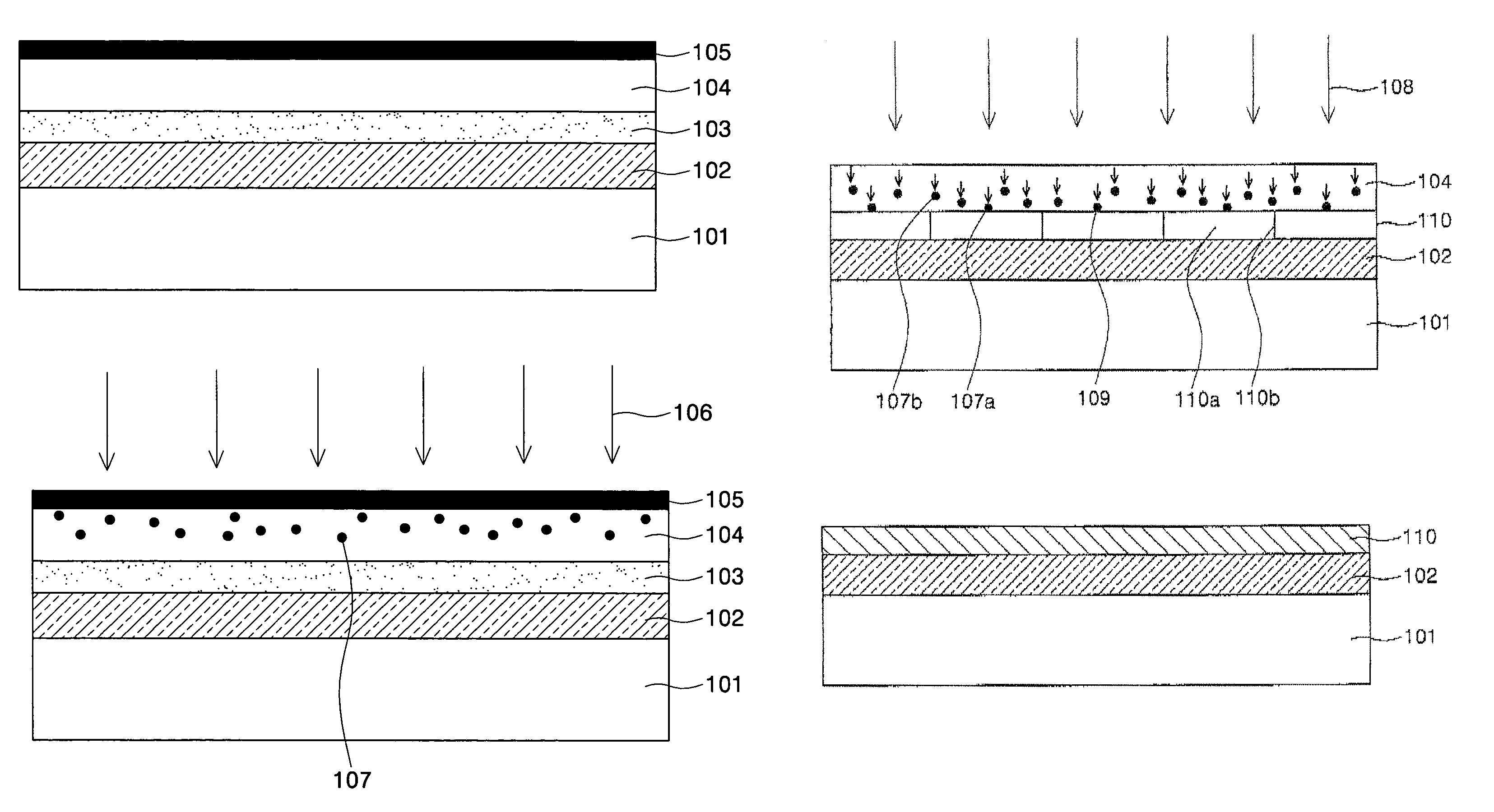
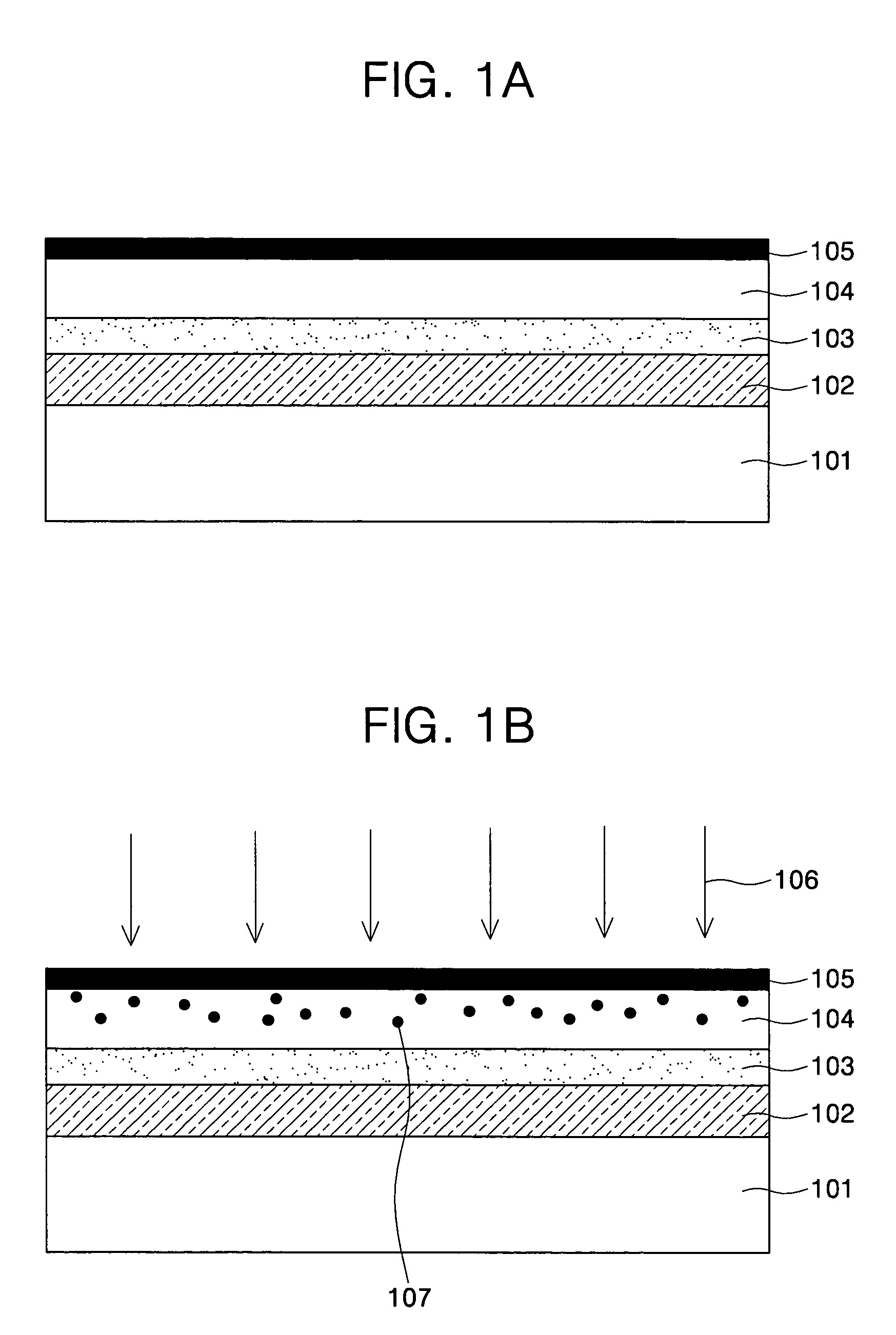
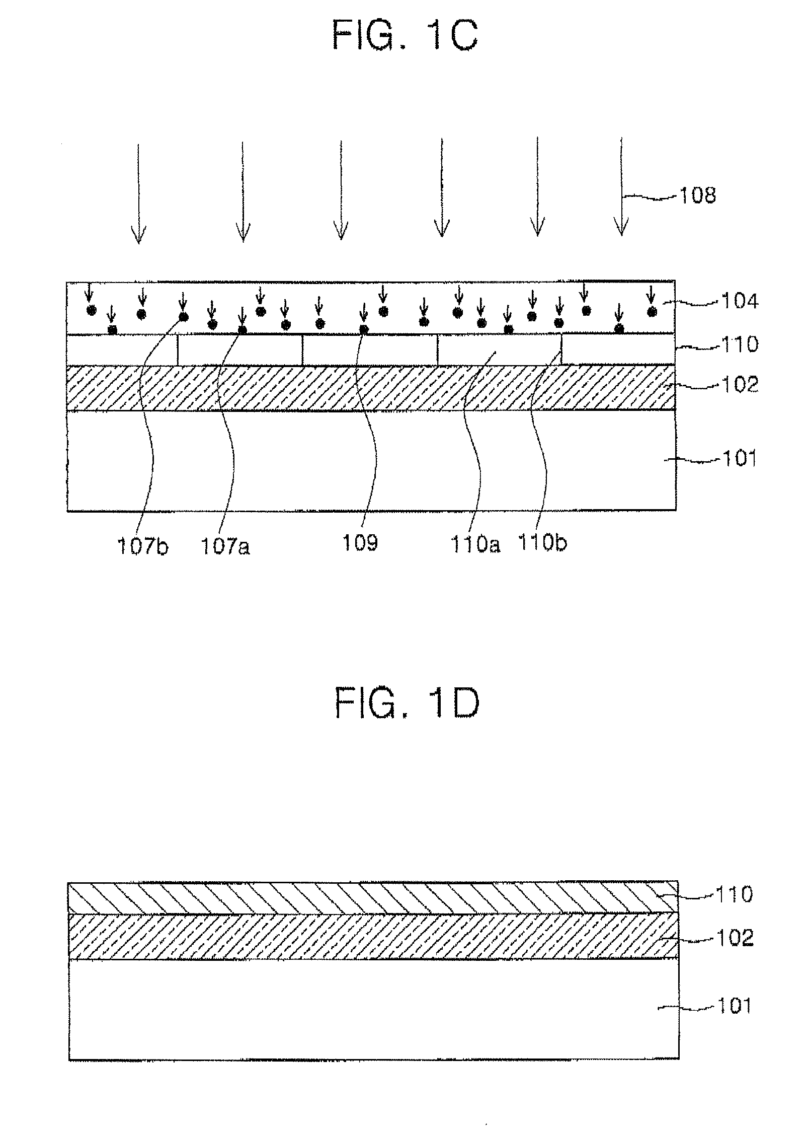
[0016]The present invention will now be described more fully hereinafter with reference to the accompanying drawings, in which exemplary embodiments of the invention are shown. In the drawings, the thickness of the layers and regions are exaggerated for clarity.

[0017]FIGS. 1A to 1D are cross-sectional views showing a process of crystallizing an amorphous silicon layer into a polycrystalline silicon layer according to the present invention.

[0018]FIG. 1A is a cross-sectional view showing a process of sequentially forming a buffer layer, an amorphous silicon layer, a capping layer and a metal catalyst layer on an insulating substrate. As shown in FIG. 1, a buffer layer 102 is formed on a transparent insulating substrate 101, such as glass or plastic, to prevent diffusion of moisture or impurities generated from the substrate or to adjust a heat transfer speed upon crystallization, such that a semiconductor layer is well crystallized.

[0019]An amorphous silicon layer 103 is then formed o...


PUM

PropertyMeasurementUnit
temperatureaaaaaaaaaa

Abstract

Disclosed is a method of fabricating a thin film transistor in which, in order to control the concentration of metal catalysts remaining on a polycrystalline silicon layer when an amorphous silicon layer formed on an insulating substrate is crystallized into the polycrystalline silicon layer by a super grain silicon (SGS) crystallization method, the substrate is annealed so that a very small amount of metal catalyst is adsorbed or diffused into a capping layer, and then a crystallization process is carried out, thereby minimizing the concentration of the metal catalysts remaining on the polycrystalline silicon layer, as well as forming a thick metal catalyst layer. The method includes preparing an insulating substrate; sequentially forming an amorphous silicon layer, a capping layer, and a metal catalyst layer on the substrate; first annealing the substrate to adsorb or diffuse metal catalysts into the capping layer; removing the metal catalyst layer; second annealing the substrate to crystallize the amorphous silicon layer into a polycrystalline silicon layer by means of the metal catalyst; and removing the capping layer. Thus, with the method of fabricating the thin film transistor of the present invention, it is possible to minimize the concentration of the metal catalysts remaining on the polycrystalline silicon layer, as well as to form a thick metal catalyst layer.

Description

CROSS-REFERENCE TO RELATED APPLICATION[0001]This application claims priority to and the benefit of Korean Patent Application No. 2004-61530, filed Aug. 4, 2004, the disclosure of which is incorporated herein by reference in its entirety.BACKGROUND OF THE INVENTION[0002]1. Field of the Invention[0003]The present invention relates to a method of fabricating a thin film transistor and, more particularly, to a method of fabricating a thin film transistor in which, in order to control the concentration of metal catalysts remaining on a polycrystalline silicon layer when an amorphous silicon layer formed on an insulating substrate is crystallized into the polycrystalline silicon layer using a super grain silicon (SGS) crystallization method, the substrate is annealed so that a very small amount of metal catalyst is adsorbed or diffused into a capping layer, and then a crystallization process is carried out.[0004]2. Description of Related Art[0005]Generally, in a thin film transistor for u...

Claims


Application Information

Patent Timeline
Patent Type & Authority Patents(United States)
IPC IPC(8): C30B28/02C30B29/06H01L21/20
CPCH01L29/66757H01L29/78675H01L21/02672H01L21/2022H01L21/3221H01L27/1277
Inventor PARK, HYE-HYANGLEE, KI-YONG
Owner SAMSUNG DISPLAY CO LTD
Why Eureka
Try Eureka