Switch linearized track and hold circuit for switch linearization
a linearization and hold circuit technology, applied in the field of analog to digital signal conversion, can solve the problems of signal dependent sampling time error, noise and non-linearity of all s/h and/or t/h circuits, and the effect of reducing the number of signals
- Summary
- Abstract
- Description
- Claims
- Application Information
AI Technical Summary
Benefits of technology
Problems solved by technology
Method used
Image
Examples
Embodiment Construction
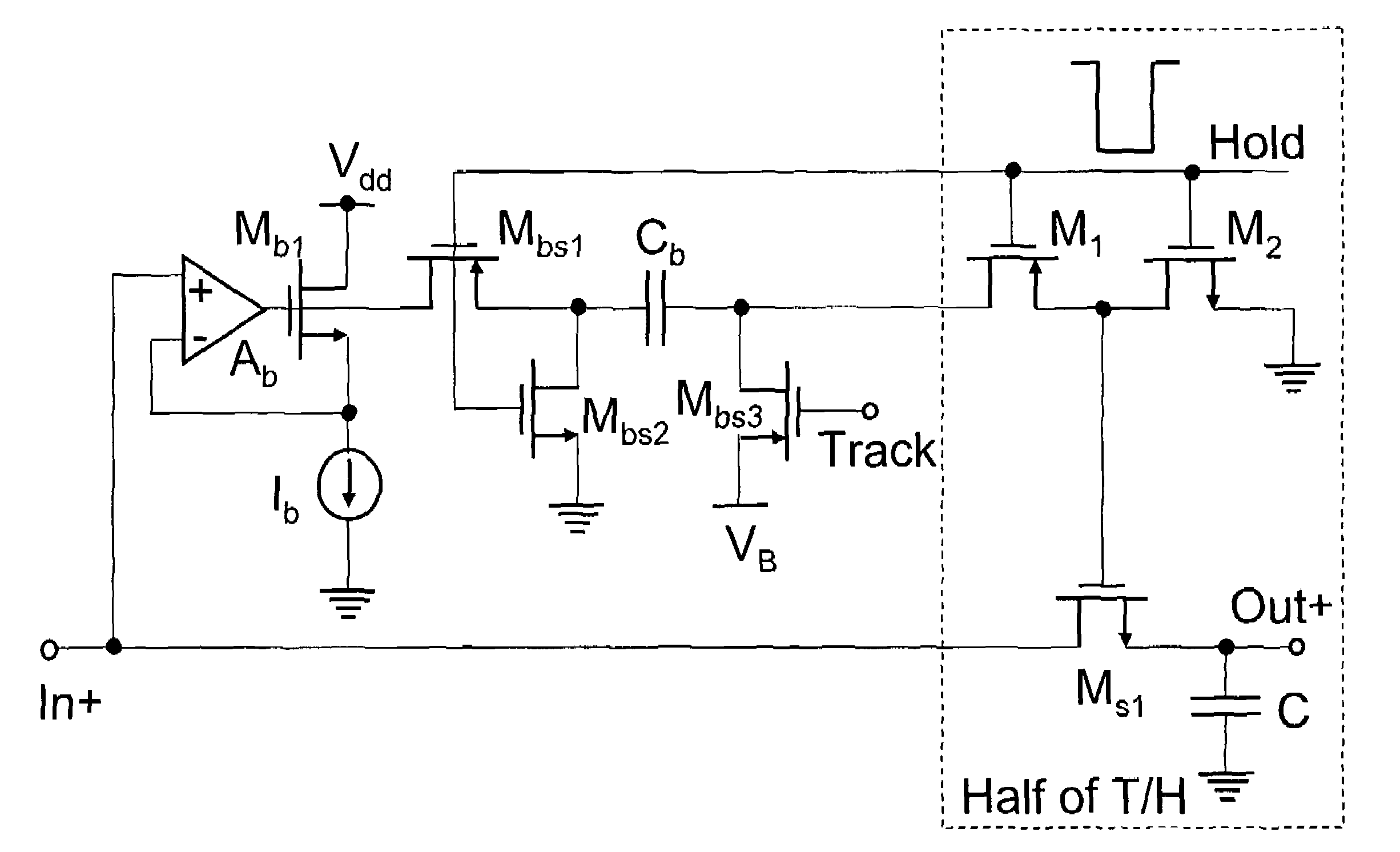
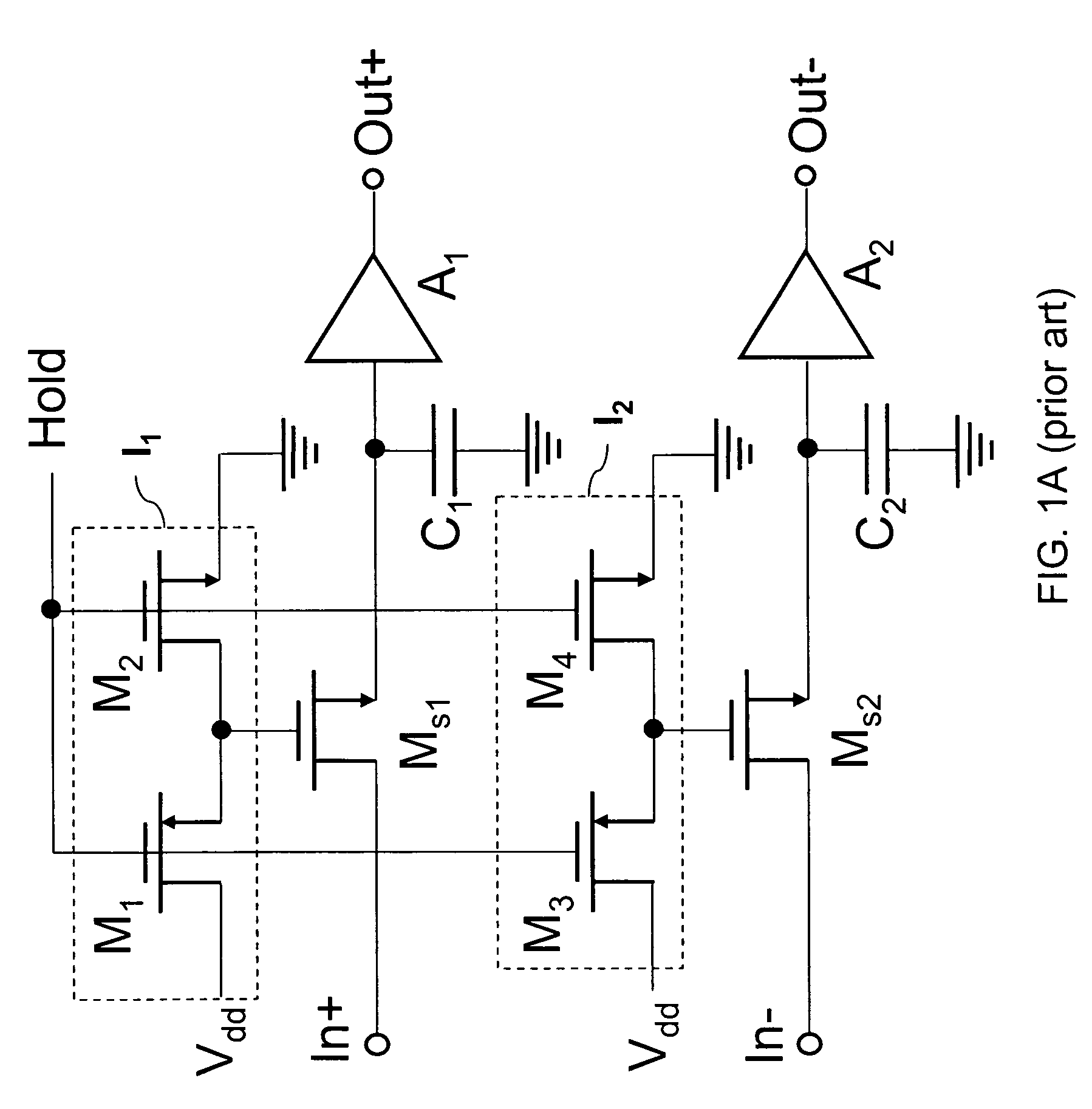
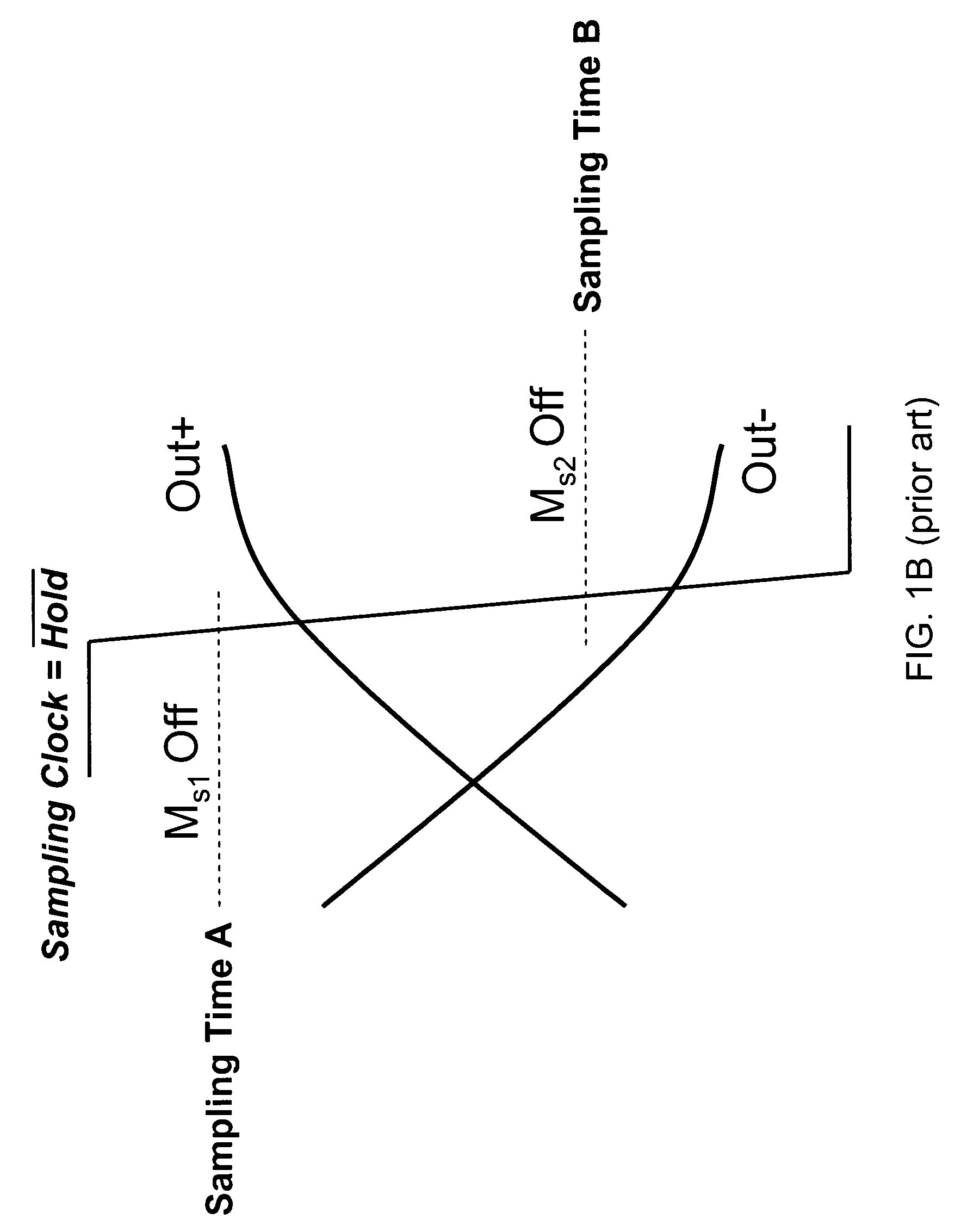
[0020]The sampling accuracy in CMOS T / H circuits is improved in embodiments of the invention by keeping switch on-resistance and channel charge injection constant. Embodiments of the invention provide CMOS T / H circuits that make the switch on-resistance and the channel charge injection linear and independent of the signal. Embodiments of the invention address problems with conventional circuits that have been identified by the present inventor. Unlike bottom-plate S / H circuits, conventional T / H circuits experience higher levels of error resulting from switch non-linearity, switch charge injection, and clock feed-through errors. In the differential T / H shown in FIG. 1A, the on-resistances of the two switches Ms1 and Ms2 vary as the input signal varies because the on-resistance is inversely proportional to the gate over-drive voltage over the threshold voltage. If this over-drive voltage is linearly proportional to the signal, the sum of the voltage drops across two switches Ms1 and M...
PUM
 Abstract
Description
Claims
Application Information


