Clock-gated model transformation for asynchronous testing of logic targeted for free-running, data-gated logic

a technology of clock-gated logic and model transformation, which is applied in the field of model transformation of clock-gated logic, can solve the problems of large number of cells, difficult physical design without the aid of computers, and complicated connections between cells

Inactive Publication Date: 2008-11-18
IBM CORP
View PDF13 Cites 3 Cited by
  • Summary
  • Abstract
  • Description
  • Claims
  • Application Information

AI Technical Summary

Benefits of technology

[0010]It is therefore one object of the present invention to provide an improved method of modeling asynchronous behavior of a circuit.
[0011]It is another object of the present invention to provide such a method which may detect asynchronous problems in a circuit which was designed for a clock-gated implementation but is carried out using a free-running, data-gated implementation.

Problems solved by technology

An IC may include a very large number of cells and require complicated connections between the cells.
Due to the large number of components and the details required by the fabrication process for very large scale integrated (VLSI) devices, physical design is not practical without the aid of computers.
As process technology scales to the deep-submicron (DSM) regime, clock-related problems such as clock skew and worst-case execution time are becoming increasingly important to the performance and reliability of IC chips and systems.
Unfortunately, when a gating term in the clock logic is driven from an asynchronous source relative to a receiving latch, it becomes much more difficult to accurately test a circuit because the receive latch may be clocked at any time after the send latch transitions.
The differences in the implementations arise from difficulties in breaking out the gating logic from the clock network.
A problem which exists in this methodology is that certain asynchronous problems are undetectable in the behavioral model which may be apparent in the gate-level model.
The testing performed on the high level model is thus inadequate for the netlist which will be synthesized.
However, when a behavioral model netlist is using a form for a clock-gated implementation and the post-synthesis netlist is using a free-running, data-gated implementation for their respective sequential elements, the post-synthesis netlist will always have a potential source of asynchronous problems.

Method used


Image

  • Clock-gated model transformation for asynchronous testing of logic targeted for free-running, data-gated logic
  • Clock-gated model transformation for asynchronous testing of logic targeted for free-running, data-gated logic
  • Clock-gated model transformation for asynchronous testing of logic targeted for free-running, data-gated logic

Examples


Embodiment Construction

)

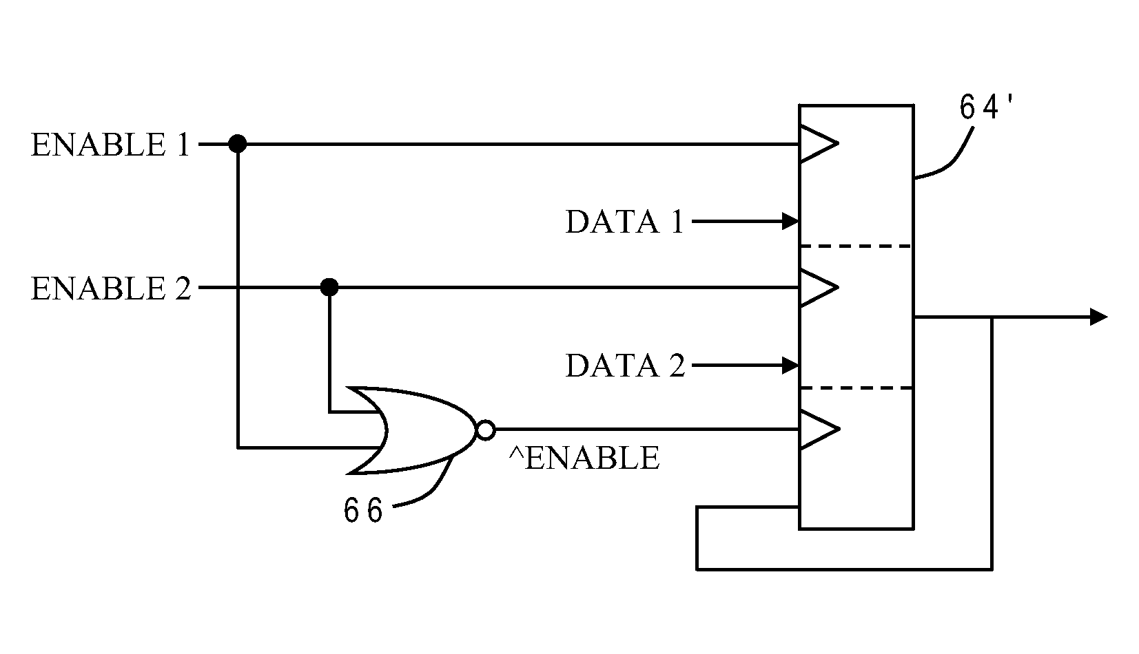
[0024]The present invention provides a novel method for modeling asynchronous behavior of a circuit, and is generally applicable to any type of digital circuit, such as execution units or memory, and clock-controlled (functional) or free-running (scan) logic. The method takes a netlist generated by conventional means and modifies latches in the netlist by adding an extra latch port to better emulate asynchronous conditions and identify potential timing problems. As explained more fully below, the present invention is particularly useful in modeling asynchronous behavior of a circuit which is clock-gated at a high-level abstraction but may be implemented as free-running, data-gated logic.

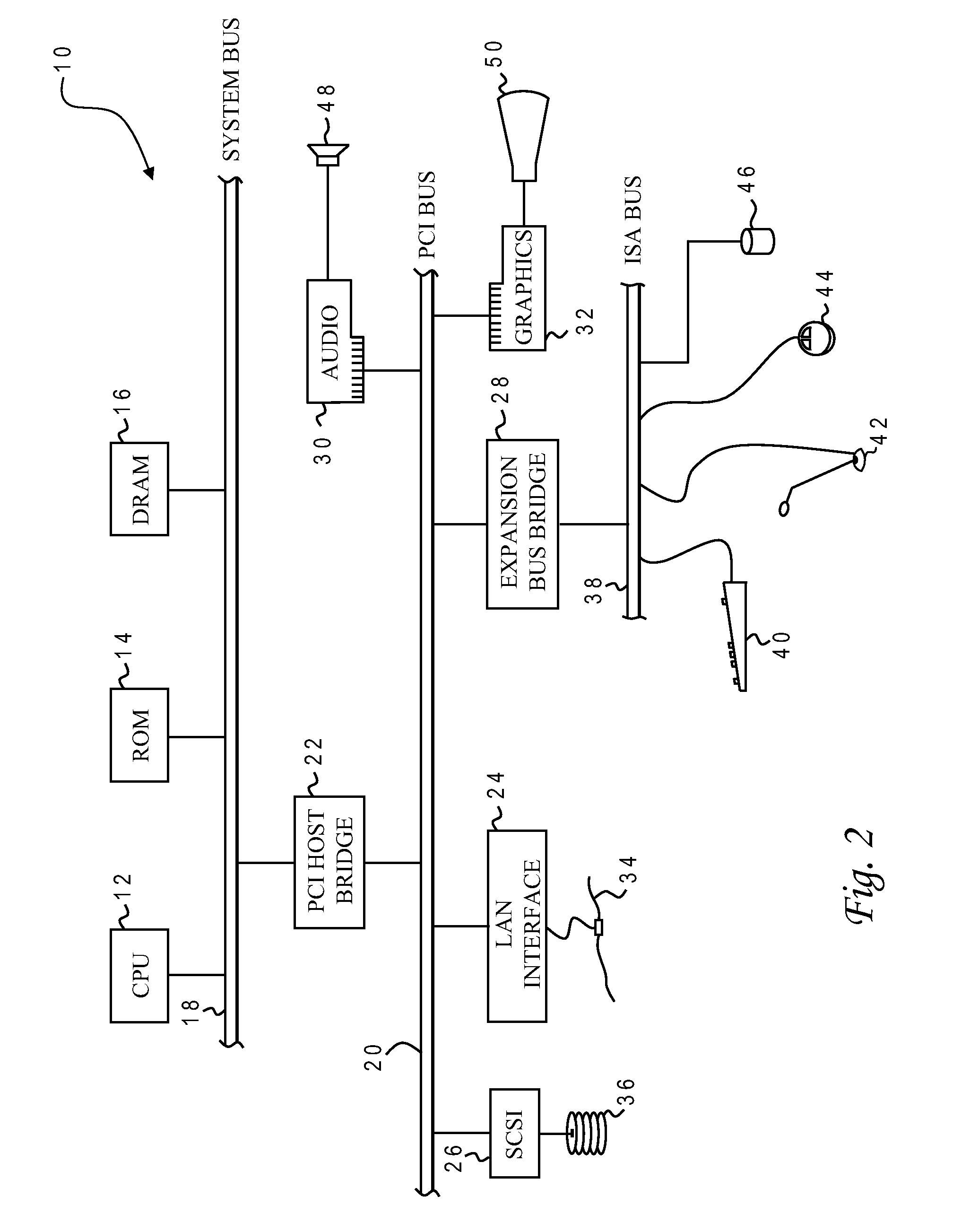
[0025]With reference now to the figures, and in particular with reference to FIG. 2, there is depicted one embodiment 10 of a computer system programmed to carry out the model transformation in accordance with one implementation of the present invention. System 10 includes a central processing unit ...


PUM


Abstract

Asynchronous behavior of a circuit is modeled by modifying latches in a netlist to add an extra port to the latches, e.g., a single-port latch is transformed into a dual-port latch. Each input port has an enable line and a data input. The data input in the added port is a feedback line from the latch output, and the enable line in the added port is the logical NOR of all of the original enable lines. By adding this extra latch port in the higher-level model, it becomes possible to introduce assertion logic to ensure that one and only one latch port for a given latch is ever active during the same simulation cycle. The model can then be tested earlier in the design methodology prior to the availability of the post-synthesis netlist. The model can also be used in both simulation and formal or semi-formal verification.

Description

BACKGROUND OF THE INVENTION[0001]1. Field of the Invention[0002]The present invention generally relates to the fabrication and design of semiconductor chips and integrated circuits, specifically to a method of modeling the operation of a circuit running under asynchronous conditions, and more particularly to a model transformation for clock-gated logic that may be implemented as free-running, data-gated logic.[0003]2. Description of the Related Art[0004]Integrated circuits are used for a wide variety of electronic applications, from simple devices such as wristwatches, to the most complex computer systems. A microelectronic integrated circuit (IC) chip can generally be thought of as a collection of logic cells with electrical interconnections between the cells, formed on a semiconductor substrate (e.g., silicon). An IC may include a very large number of cells and require complicated connections between the cells. A cell is a group of one or more circuit elements such as transistors,...

Claims


Application Information

Patent Timeline
Patent Type & Authority Patents(United States)
IPC IPC(8): G11C8/00
CPCG06F17/5022G06F17/504G06F2217/62G06F30/33G06F30/3323G06F30/396G06F30/3308G06F2117/04
Inventor JA, YEENELSON, BRADLEY S.ROESNER, WOLFGANG
Owner IBM CORP
Why Eureka
Try Eureka