System and method for compensating for PVT variation effects on the delay line of a clock signal

a clock signal and delay line technology, applied in the field of electronic data storage, can solve problems such as mapping errors, limit the speed of read operations, and the current implementation of master-to-slave systems may have stringent duty cycle requirements

Inactive Publication Date: 2008-11-18
AVAGO TECH WIRELESS IP SINGAPORE PTE
View PDF5 Cites 12 Cited by
  • Summary
  • Abstract
  • Description
  • Claims
  • Application Information

AI Technical Summary

Benefits of technology

[0008]The present invention utilizes the advantages of the Master-Slave and Data-path switching approaches without suffering from any of the disadvantages. The present invention provides a method for compensating for process, voltage, and temperature variation without complex online / offline swapping of data paths which require a dedicated FIFO (First-in First-out) buffer design. The present invention does not require an embedded FIFO and can therefore interface to standard FIFO designs used in most memory controllers.

Problems solved by technology

The delay of the clock relative to the arrival time of the data at the sampling point may be subject to process, voltage and temperature (PVT) variation, which may limit the speed of read operations.
However, the current solutions may introduce mapping errors due to on-chip process variation from the Master to Slave delays.
In addition, the currently implemented Master-to-Slave systems do not account for internal skew across multiple data paths which are strobed with a single clock.
Still further, the currently implemented Master-to-Slave systems may have stringent duty cycle requirements.
However, this method does not support passing of the strobed data directly to a standard FIFO (first-in first-out) buffer that is common in memory controllers.
This FIFO design is specific to patent application Ser. No. 11 / 523,139 and wilt not always be desirable in all memory controller designs.

Method used


Image

  • System and method for compensating for PVT variation effects on the delay line of a clock signal
  • System and method for compensating for PVT variation effects on the delay line of a clock signal
  • System and method for compensating for PVT variation effects on the delay line of a clock signal

Examples


Embodiment Construction

[0013]Reference will now be made in detail to the present invention, examples of which are illustrated in the accompanying drawings.

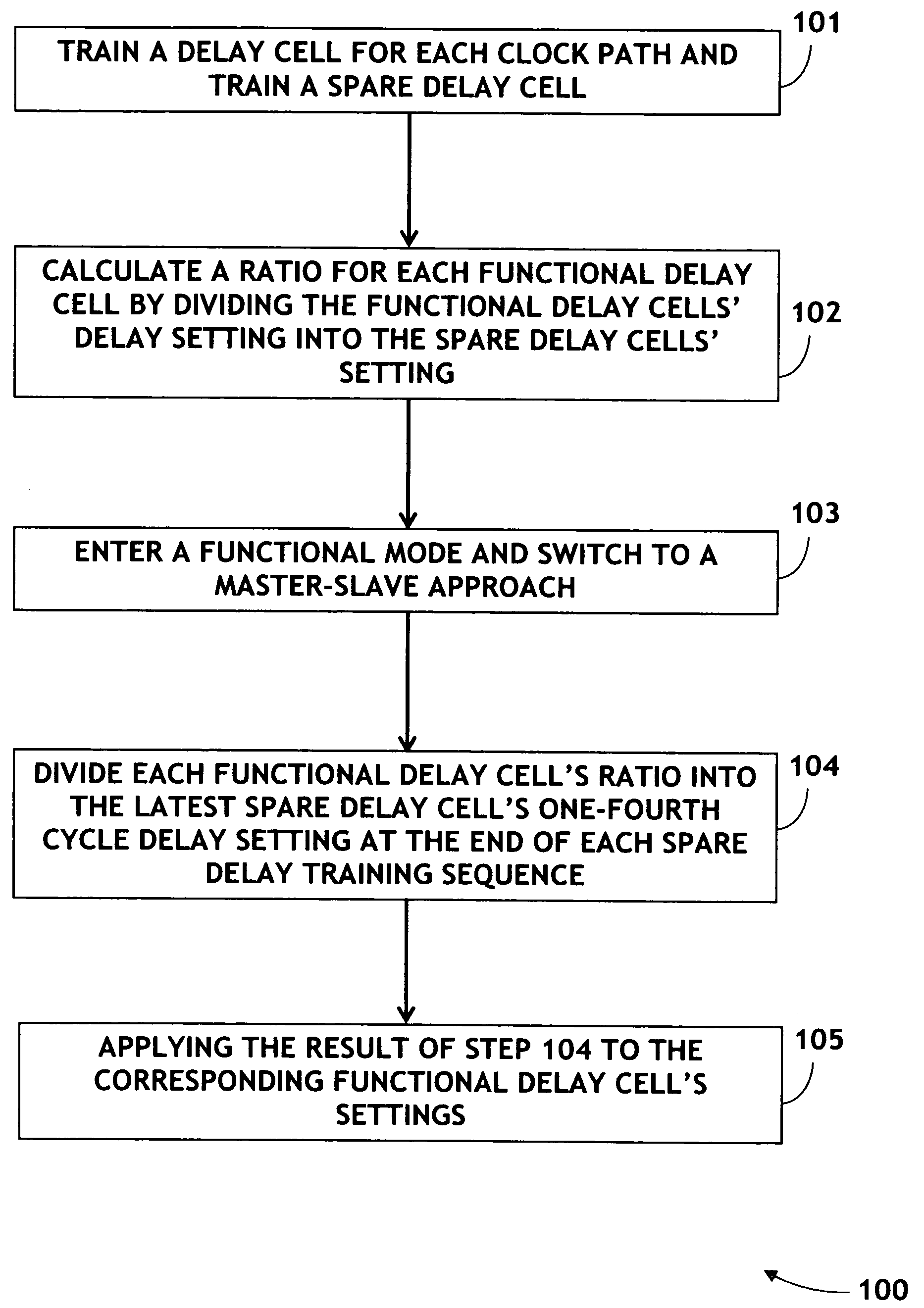
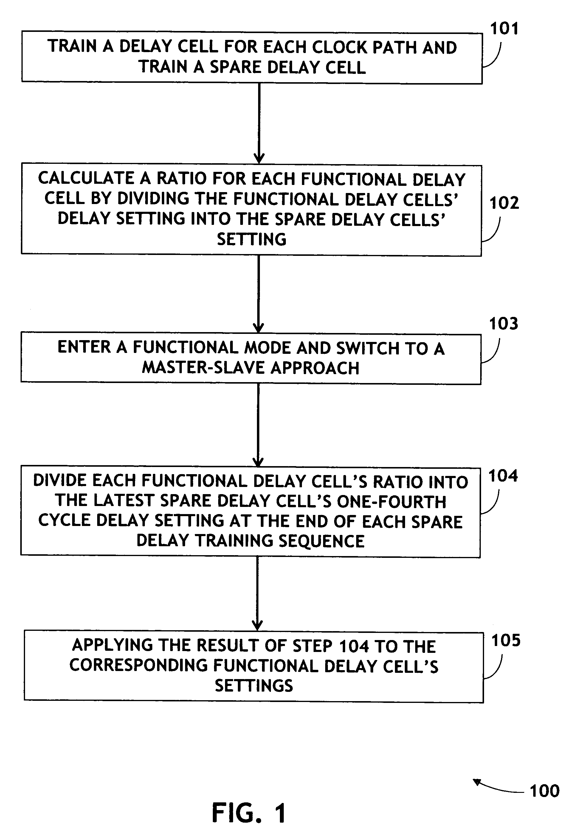
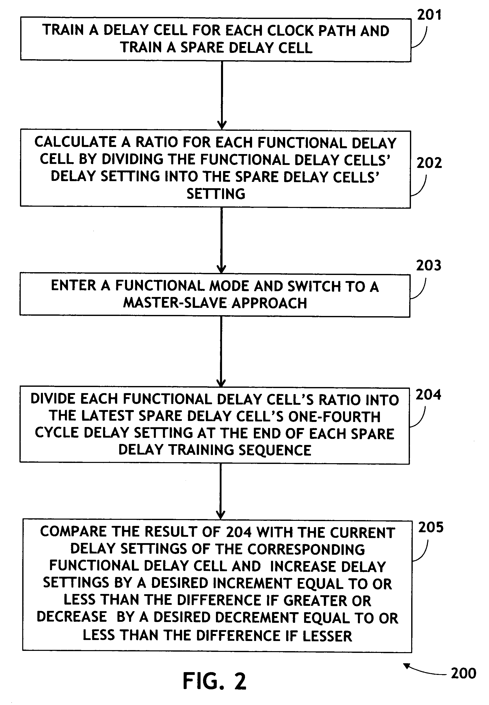
[0014]Referring to FIG. 1, a method 100 for process, voltage, and temperature compensation in accordance with an exemplary embodiment of the present invention is shown. The method 100 includes the step 101 of training a delay cell for each clock path (namely a Functional delay) and training a spare delay cell in similar method to the training described in patent application Ser. No. 11 / 523,139. The method includes training each delay cell in parallel. Training a delay cell may include adding an offset delay to the determined aligned or ¼ delay settings The method 100 further includes the step 102 of calculating a ratio for each Functional delay cell by dividing the Functional delay cells' delay setting into the spare delay cells' one-fourth cycle setting. A ratio value other than 1.0 reflects any difference between each delay cell and the spare delay ce...


PUM


Abstract

The present invention is directed to a method for compensating for process, voltage, and temperature variation without complex online / offline swapping of data paths requiring a dedicated FIFO(First-in First-out) buffer design. Delay cells are trained for each clock path (namely a Functional delay) and a spare delay cell is trained. A ratio is calculated for each Functional delay cell by dividing the Functional delay cells' setting into the spare delay cells' one-fourth cycle setting. These ratios reflect any process variation. Functional mode is then entered and a Master-Slave approach switched to, during which the spare delay cell repeats the training sequence continuously while the Functional delay cells delay the clocks from the RAM(Random Access Memory). Each Functional delay cell is updated at the end of each training sequence of the spare delay cell, compensating for voltage and temperature change, by dividing the ratio into the new spare delay cell one-fourth cycle setting.

Description

FIELD OF THE INVENTION[0001]The present invention relates to the field of electronic data storage and particularly to a system and method for providing process, voltage, and temperature compensation.BACKGROUND OF THE INVENTION[0002]A read path of a RAM (Random-access Memory) device may require a delay to be added to a clock path to strobe data in the center of an eye pattern. The delay of the clock relative to the arrival time of the data at the sampling point may be subject to process, voltage and temperature (PVT) variation, which may limit the speed of read operations. A method may be utilized for first removing process variation. Further updates may be applied to remove voltage variation and temperature variation.[0003]Current solutions may utilize a Master delay cell to emulate a correct delay setting. The correct delay setting may then be applied to Slave delay cells within the actual clock path. The Master delay cell may then be monitored for voltage and temperature changes, ...

Claims


Application Information

Patent Timeline
Patent Type & Authority Patents(United States)
IPC IPC(8): G06F3/00
CPCG06F1/10G11C7/04G11C7/22G11C7/222G11C7/227G11C29/02G11C29/023G11C29/028G11C2207/2254
Inventor MAGEE, TERENCEHUGHES, THOMASKONG, CHENG-GANG
Owner AVAGO TECH WIRELESS IP SINGAPORE PTE
Why Eureka
Try Eureka