

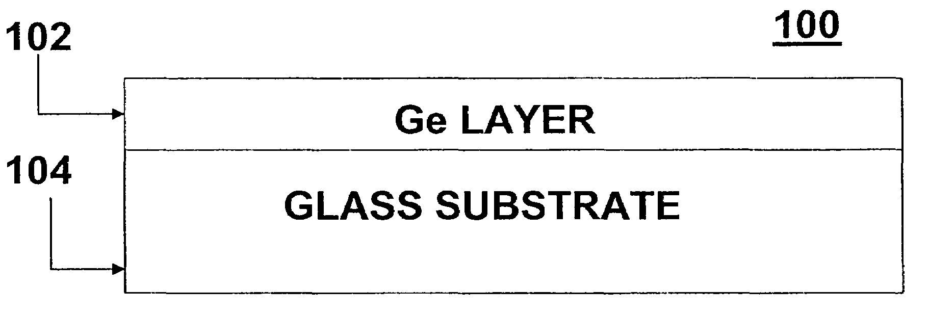
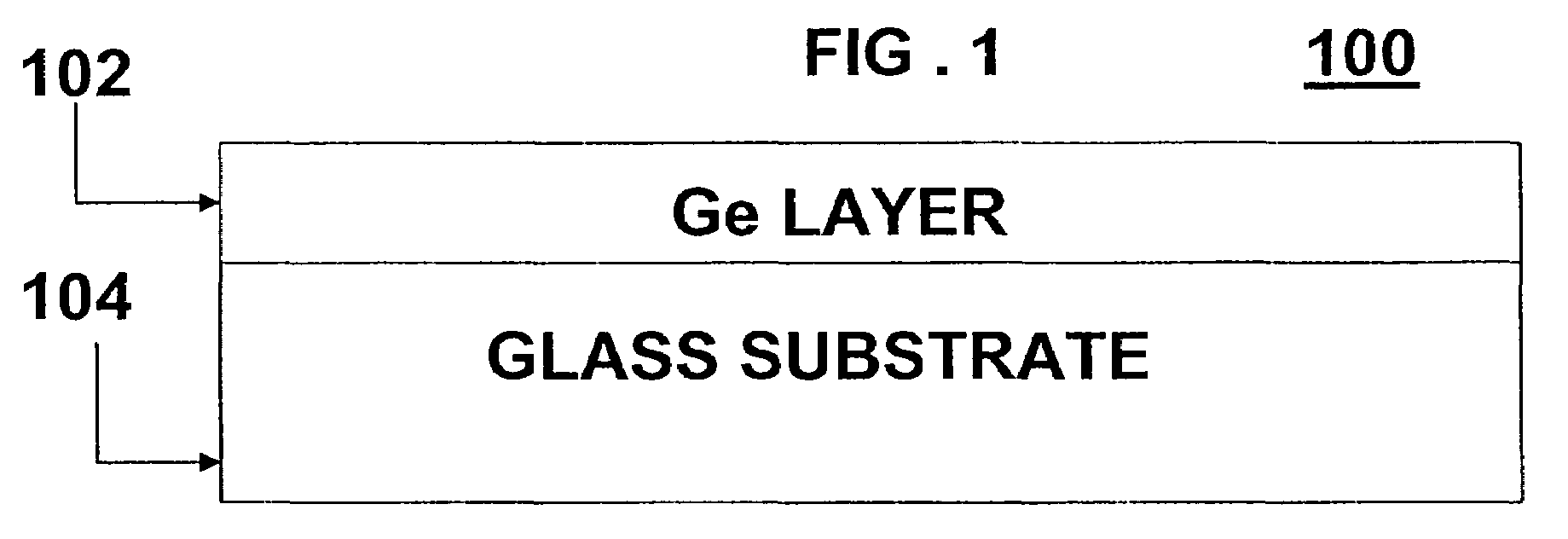
Germanium on glass and glass-ceramic structures
a technology of glass or glassceramic and germanium, applied in the direction of basic electric elements, electrical apparatus, semiconductor devices, etc., can solve the problems of cost and/or bond strength and durability, cost of silicon wafers, cost of support substrates,
- Summary
- Abstract
- Description
- Claims
- Application Information
AI Technical Summary
Benefits of technology
Problems solved by technology
Method used
Image

Examples
example 1
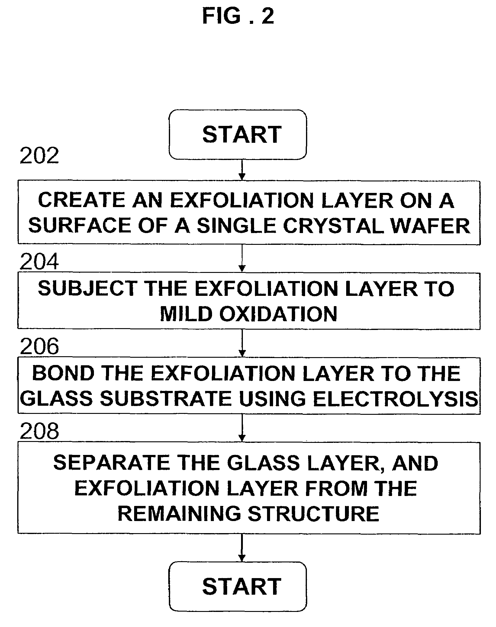
[0066]A Germanium wafer () exhibiting a 100 mm diameter and a thickness of 500 microns thick was subjected to a hydrogen ion implantation process which involved utilizing a dosage of 4×10¹⁶ ions / cm2 and implantation energy of 100 KeV. The wafer was then treated in oxygen plasma, under standard conditions, for a period of 10 minutes so as to oxidize the surface groups. An alkali aluminoborosilicate glass wafer having a composition (in weight percent) as follows was provided:
64.1% SiO2, 8.4% B2O3, 4.2 Al2O3, 6.4 Na2O, 6.9K2O, 5.9 ZnO 4.0 TiO2, 0.1 Sb2O3.
The glass exhibited a 100 mm diameter, a linear thermal CTE matched to that of Germanium, and a strain point of 529° C. The glass wafer was washed with Fischer scientific Contrad 70 detergent in ultrasonic bath for 15 minutes followed by distilled water wash for 15 minutes in ultrasonic bath. The glass wafer was thereafter washed in 10% nitric acid, again followed by distilled water wash. Both these wafers were finally cleaned in a spi...
example 2
[0068]The above experiment was repeated with an alkaline earth aluminosilicate glass (particularly a calcium aluminosilicate glass exhibiting the Example 8 composition as described above) wafer without any alkali present in the composition. The glass exhibited a strain point of 735° C. and again exhibited a CTE which matched that of the Ge wafer. In this case, again an excellent Ge defect-free thin film (0.5 μm ) transfer to glass was obtained, which was evidence of the fact that the presence of alkali ions in the glass in the compositions is not necessary.
PUM
| Property | Measurement | Unit |
|---|---|---|
| strain point | aaaaa | aaaaa |
| strain point | aaaaa | aaaaa |
| thickness | aaaaa | aaaaa |
Abstract
Description
Claims
Application Information