Ceramic substrate grid structure for the creation of virtual coax arrangement

a ceramic substrate and grid structure technology, applied in the field of substrates, can solve the problems of increasing the contribution of coupled noise, reducing the number of connected noise interactions, and increasing the need for operation at higher frequencies, so as to reduce the interaction of coupled noise and minimize the effect of wirability problems

Inactive Publication Date: 2008-12-16
GLOBALFOUNDRIES INC
View PDF13 Cites 9 Cited by
  • Summary
  • Abstract
  • Description
  • Claims
  • Application Information

AI Technical Summary

Benefits of technology

[0003]In the present invention, the coupled noise for the x, y and z interconnects is controlled by reducing signal density by adding EM (Electromagnetic) shielding to the traces (that is, to the conductive paths). In the present invention a manufacturable geodetic approach is employed as a solution of the problem. The structure of the present invention reduces the coupled noise interaction for both the vertical and the x-y plane interconnects by a factor of from four to six, while at the same time minimizing wirability problems.
[0004]The solution proposed herein creates a virtual coax (that is, coaxial conductor) arrangement for the vertical signal interconnections and by doing so it allows their operation at a data rate that is two to three times higher than existing technology.
[0005]A central aspect of the present invention is the replacement of the usual orthogonal grid array currently used for the power supply planes of glass ceramic substrate modules by a geodetic structure of equilateral triangles implemented trough the use of rhomboid shapes so that the manufacturing complexity is not increased. Specific spacing of these shapes allows their construction within the current ground rules of ceramic technology. The displacement of the rhombus shapes among the different planes minimizes the loss of wiring density, while at the same time it reduces the coupled noise by a factor of four. In addition, calculations indicate that the proposed structure reduces the average interconnect latency by 16.6%.

Problems solved by technology

It is well known that with the continuing shrinkage of electronic circuit components, there is a concomitant need for operation at higher frequencies.
At these higher frequencies, cross coupling between physically adjacent conductive paths becomes a greater problem.
However, this makes the contribution of the coupled noise, to support the higher data rates, even more pronounced.

Method used


Image

  • Ceramic substrate grid structure for the creation of virtual coax arrangement
  • Ceramic substrate grid structure for the creation of virtual coax arrangement
  • Ceramic substrate grid structure for the creation of virtual coax arrangement

Examples


Embodiment Construction

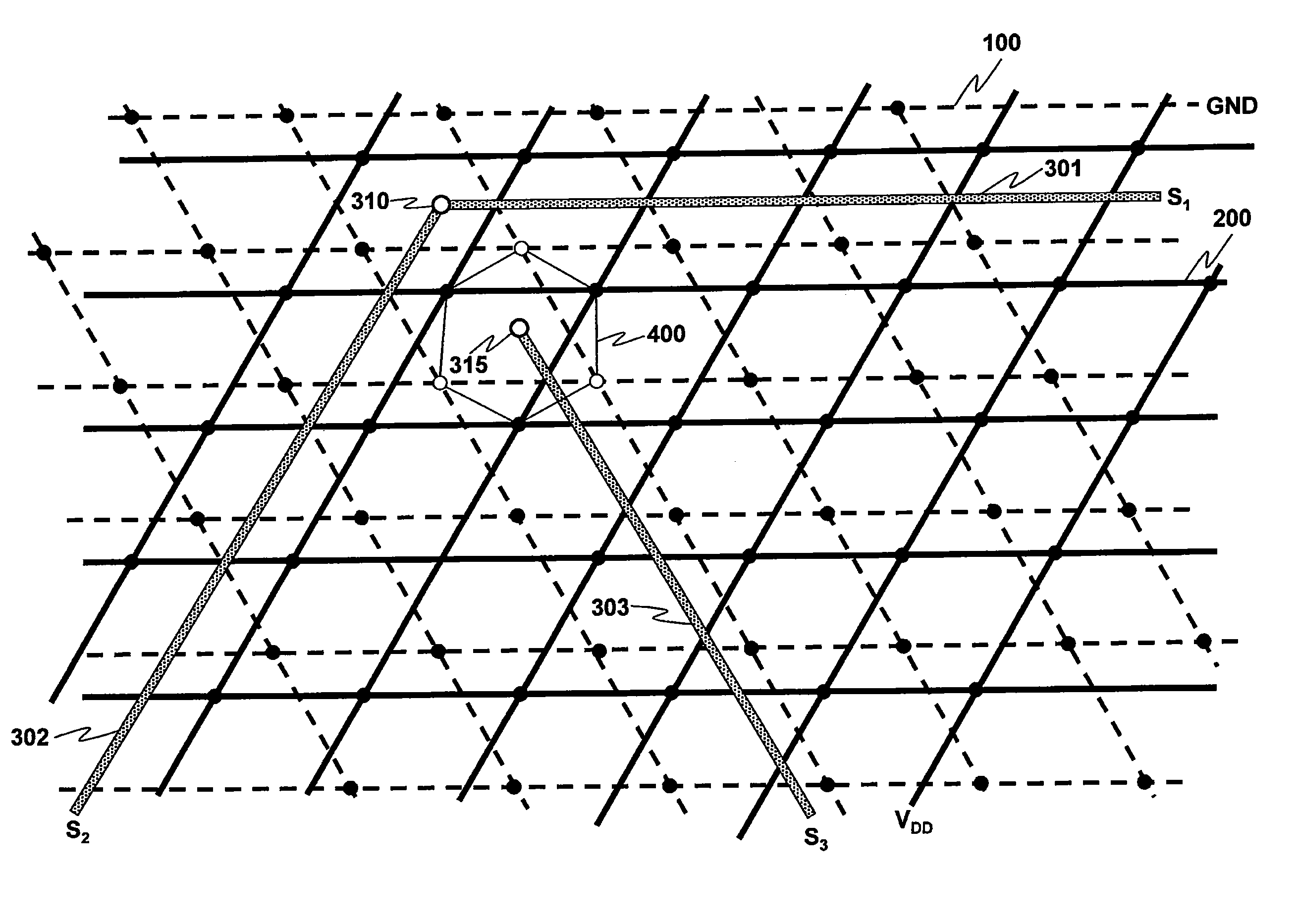
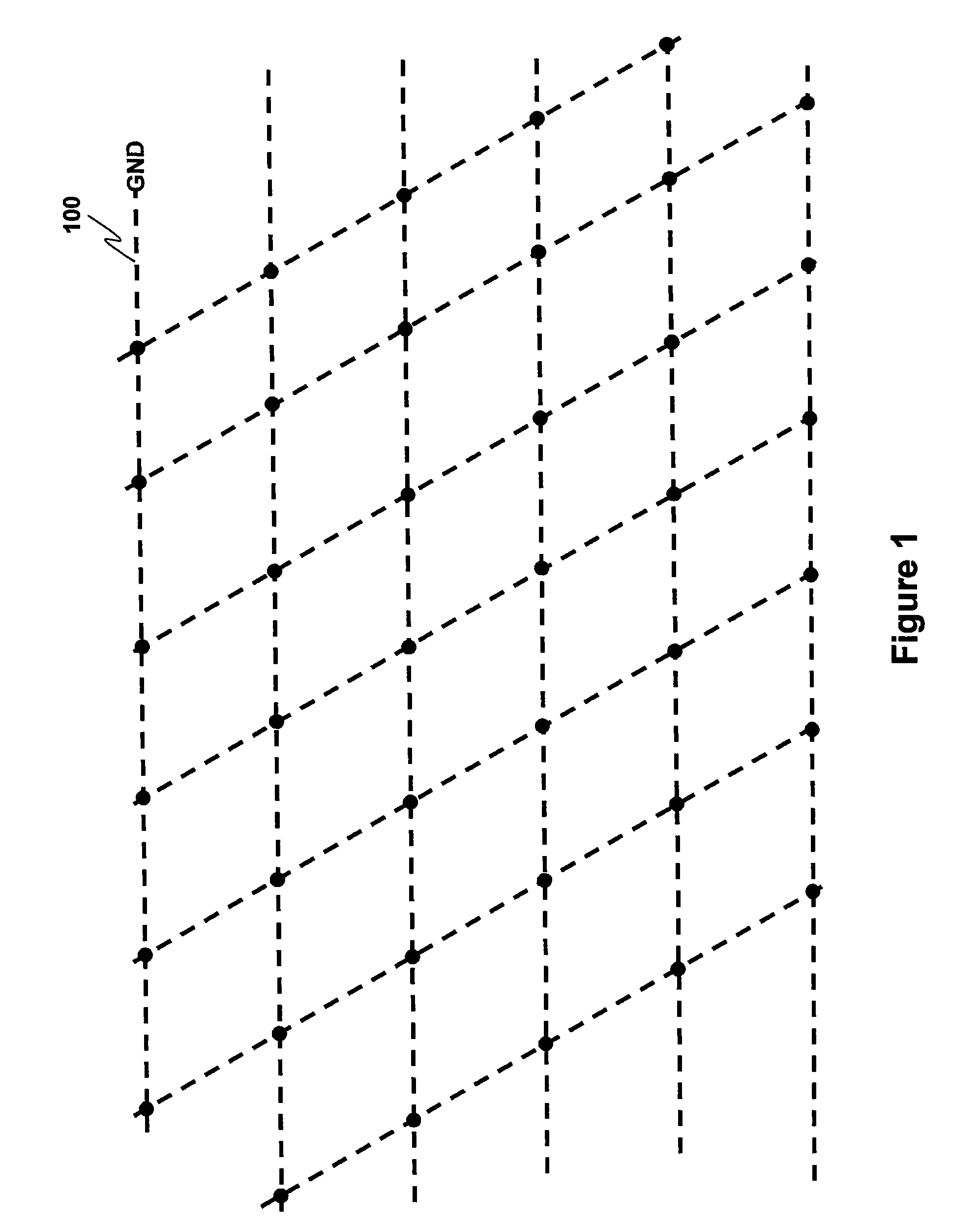
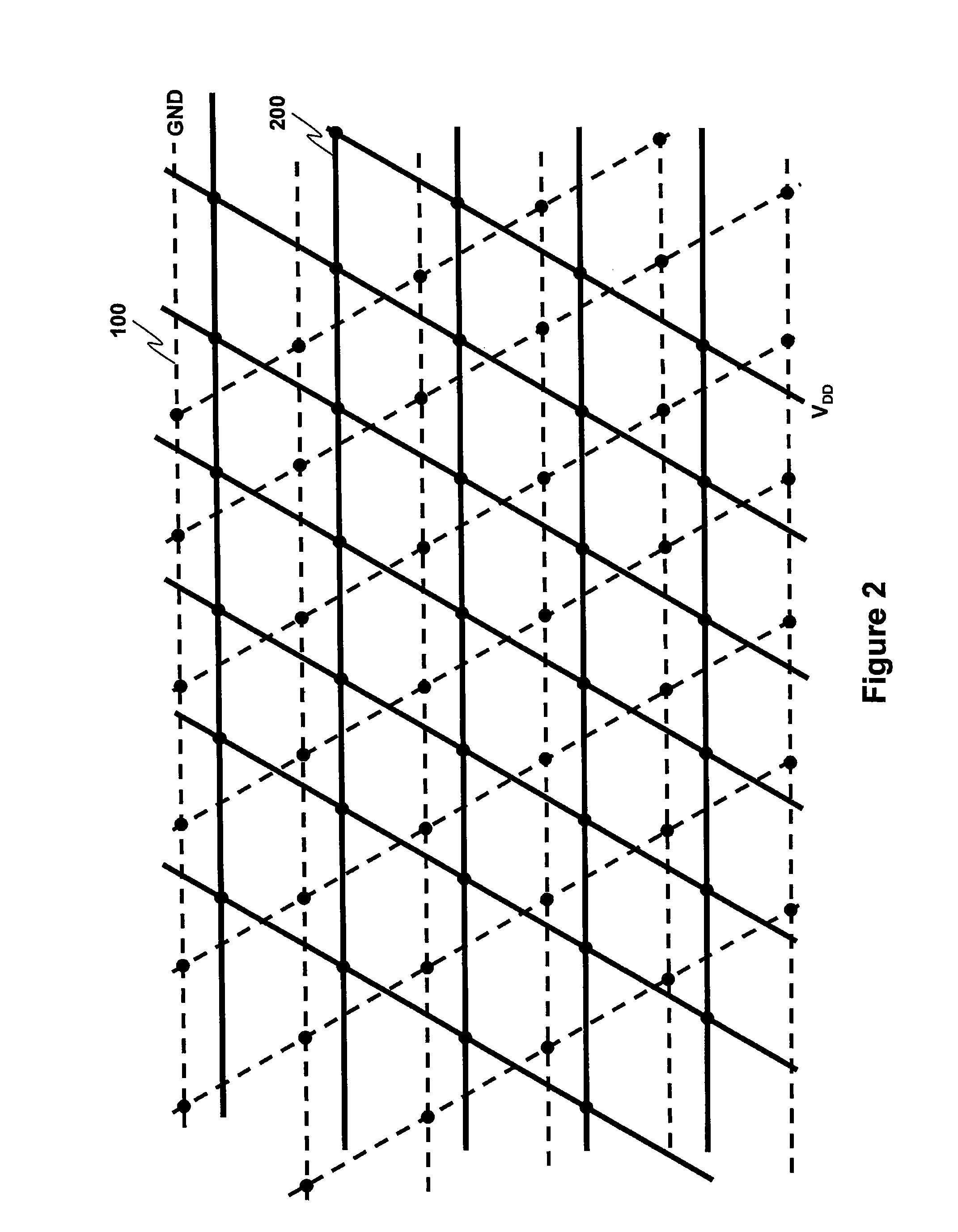
[0020]FIG. 1 is a top view of the patterns of conductive lines in one of the layers of a substrate used for providing the ground voltage to the interconnected circuit chips. For illustrative purposes only, this particular layer is referred to a ground plane or ground plane layer. Typically, one of these substrates includes a plurality of layers having various patterns of conductors. In conventional substrate designs these conductors are arranged in orthogonal patterns. In such substrates there are typically three different kinds of layers: ground plane layers, power plane layers and signal layers. The signal layers are typically found between a ground plane layer and a power plane layer. However, there is no hard and fast rule specifying the number of signal layers present.

[0021]For purposes of illustration, it is assumed that the layer shown in FIG. 1 is a ground plane layer and it is designated by reference numeral 100. It is a significant feature of the present invention is that ...


PUM

PropertyMeasurementUnit
conductiveaaaaaaaaaa
electrical poweraaaaaaaaaa
frequenciesaaaaaaaaaa

Abstract

Signal line conductors passing through vertical vias in an insulative substrate for supporting and interconnecting integrated circuit chips are provided with shielding conductors in adjacent vias that link respective power and ground planes. The shielding conductors' presence in positions around a signal via is made possible through the employment of power plane and ground plane conductive grids that are laid out in rhomboid patterns. The power plane and ground plane grids possess a left-right mirror relation to one another and are displaced to place the rhomboid's corners to avoid overlapping any of the grid lines.

Description

TECHNICAL FIELD[0001]This invention relates in general to substrates to which integrated circuit chips are affixed so as to provide interconnectivity between the chips and with other circuits and systems external to the substrate. More particularly, the present invention is directed to a to a configuration of ground plane and power plane conductors which reduce cross coupling, lowers losses and permits higher frequency operation. Even more particularly, the present invention is directed to a configuration of conductive via paths which act essentially as a coaxial shielding arrangement. (A “via” is a vertical path in the substrate through which conductive material therein carries electrical power and signals.) It is also noted that the present invention is particularly useful with glass ceramic substrates; however, the conductive configurations of the present invention are employable in conjunction with any insulative substrate material including polymeric materials.BACKGROUND OF THE...

Claims


Application Information

Patent Timeline
Patent Type & Authority Patents(United States)
IPC IPC(8): H05K1/03
CPCH05K1/0219H05K1/0224H01L23/49827H01L23/49822Y10T29/49155H01L23/49838H01L2223/6622H01L2924/09701H05K1/0253H05K2201/09609H05K2201/09618H05K2201/09681H01L2924/0002Y10T29/4913Y10T29/49128Y10T29/49126H01L2924/00
Inventor BECKER, WIREN D.CHEN, ZHAOQINGKATOPIS, GEORGE
Owner GLOBALFOUNDRIES INC
Why Eureka
Try Eureka