Method and apparatus for process control with in-die metrology

a process control and metrology technology, applied in the direction of electrical testing, instruments, electric digital data processing, etc., can solve the problems of difficult to align the substrate and position the proxies within such a small spot size, and the number of features that can be examined is generally destroyed

Active Publication Date: 2008-12-23
TEVET PCT
View PDF13 Cites 98 Cited by
  • Summary
  • Abstract
  • Description
  • Claims
  • Application Information

AI Technical Summary

Problems solved by technology

Unfortunately, the substrate is generally destroyed by cutting.
Moreover, the number of features that can be examined may be limited to features lying along the cut.
However, it can be difficult to align the substrate and position the proxies within such a small spot size.
Unfortunately, features in the proxies may not be representative of features in the dies.
However, the SEM beam may burn areas of the substrate, and alignment of the small SEM beam may be difficult and / or time consuming.

Method used


Image

  • Method and apparatus for process control with in-die metrology
  • Method and apparatus for process control with in-die metrology
  • Method and apparatus for process control with in-die metrology

Examples


Embodiment Construction

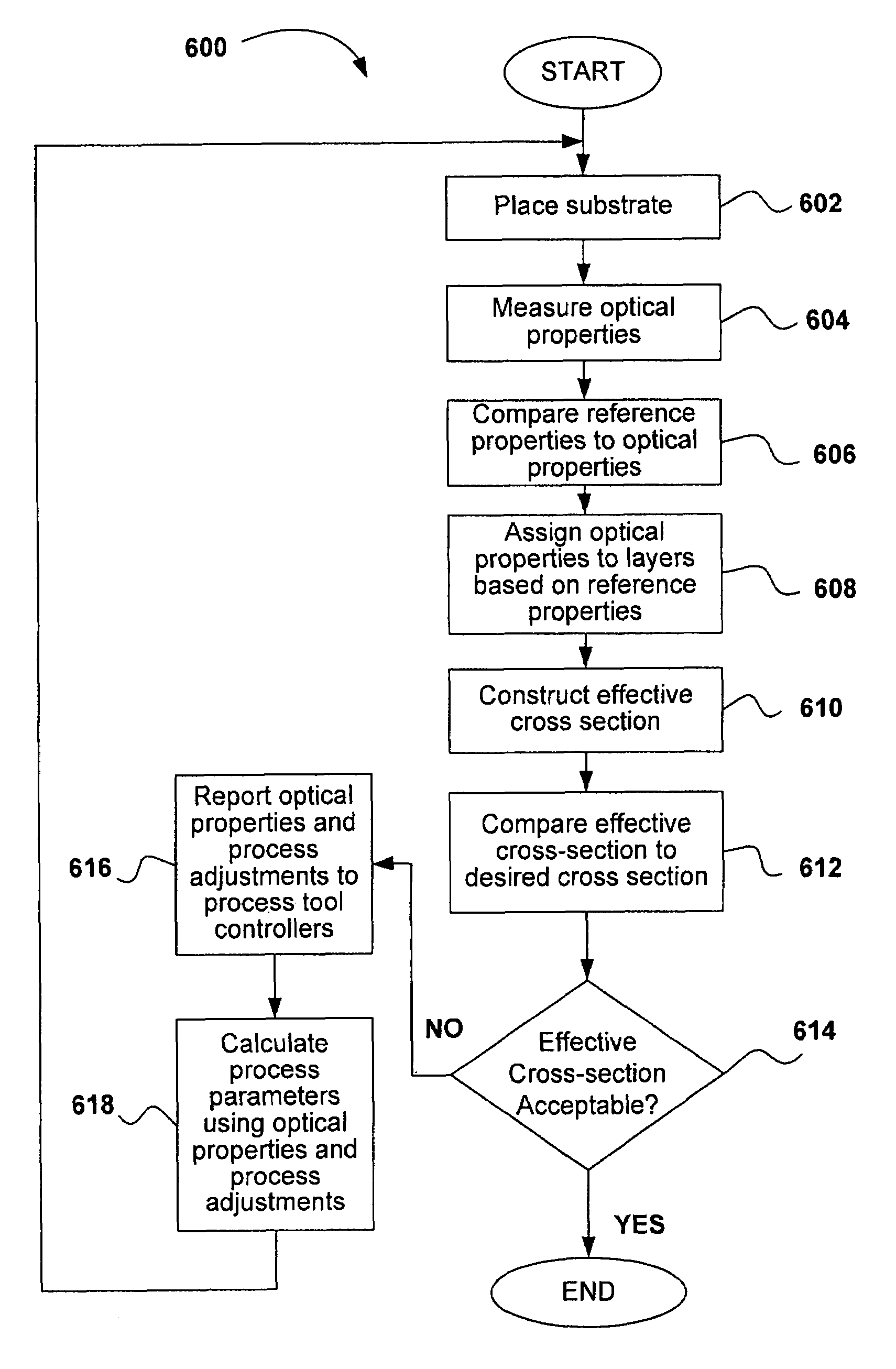
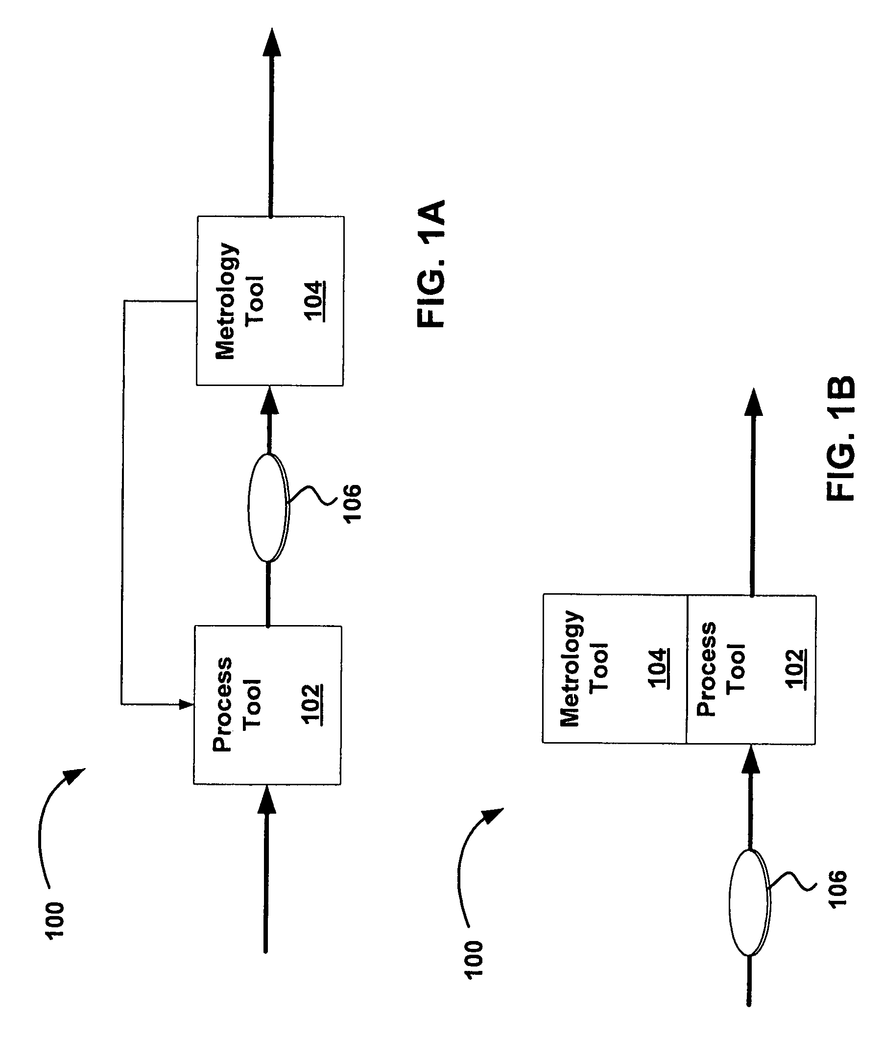
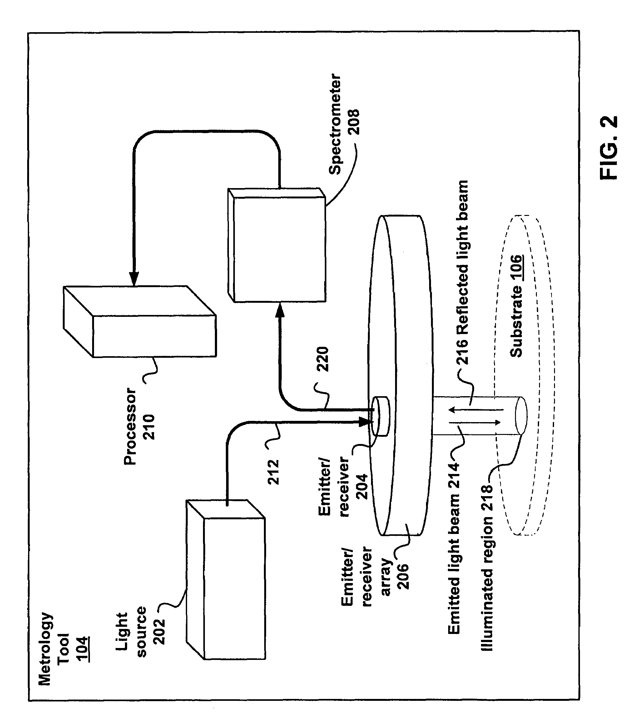
[0024]FIG. 1A is a block diagram illustrating an environment 100 for processing a substrate 106. The processing environment 100 includes a process tool 102 and a metrology tool 104. The substrate 106 may include a silicon wafer, a photolithographic mask, a gallium arsenide wafer, a germanium wafer, etc. The process tool 102 is configured to perform a process on the substrate 106. For clarity, only one process tool 102 is illustrated in FIG. 1A; however, a person of ordinary skill in the art would understand that multiple process tools 102 may each perform one or more processes on the layer of the substrate 106. A typical substrate may include one or more semiconductor devices arranged on the substrate as an array of one or more dies, while a typical semiconductor device may include multiple layers (e.g., source layer, drain layer, capacitor layer, resistor layer, gate layer, contact pad layer, conductor layer, etc.). Typical processes, include deposition of material onto the substra...


PUM


Abstract

Various embodiments include a method for providing instructions to a process tool. The method includes emitting an incident light beam at a substrate, receiving a reflected light beam from the substrate and determining a spectrum of the reflected light beam. The method further includes determining a first property of a first layer of the substrate and a second property of a second layer of the substrate, based on the spectrum determination. The method further includes comparing the first property of the first layer to a first reference property and comparing the second property of the second layer to a second reference property. The method further includes determining the instructions based on the first property comparison and the second property comparison; and providing the instructions to the process tool.

Description

CROSS-REFERENCE TO RELATED APPLICATIONS[0001]The present application incorporates by reference U.S. Provisional Patent Application Ser. No. 60 / 816,815 filed on Jun. 26, 2006 for “Integrating a Metrology Instrument for Multi-film Testing,” U.S. Provisional Patent Application Ser. No. 60 / 817,014 filed on Jun. 26, 2006 for “Thickness and Optical Property of a Multi-film Stack Using Wavelength Illumination Filtering for Film Separation,” and U.S. Provisional Patent Application Ser. No. 60 / 816,893 filed on Jun. 26, 2006 for “System and Methods for Single Wafer Process Control.”BACKGROUND OF THE INVENTION[0002]1. Field of the Invention[0003]The present invention relates to semi-conductor manufacturing equipment and more particularly a method and apparatus for providing instructions to process tools.[0004]2. Description of Related Art[0005]Semiconductor manufacturing involves various steps such as adding material to a layer, removing material from a layer or modifying a layer of a substrat...

Claims


Application Information

Patent Timeline
Patent Type & Authority Patents(United States)
IPC IPC(8): G06F19/00
CPCG01B11/0625
Inventor DU-NOUR, OFER
Owner TEVET PCT
Why Eureka
Try Eureka