Designing an integrated circuit to improve yield using a variant design element

a variant design element and integrated circuit technology, applied in the field of chip design, can solve the problems of difficult to reduce the failure rate of these attributes to acceptable levels, design rule documents no longer suffice, and extremely complex manufacturing process of integrated circuit fabrication, so as to achieve rapid and effective realization of significant yield improvement, the effect of reducing or eliminating relian

Inactive Publication Date: 2009-02-03
PDF SOLUTIONS INC
View PDF9 Cites 181 Cited by
  • Summary
  • Abstract
  • Description
  • Claims
  • Application Information

AI Technical Summary

Benefits of technology

[0013]The approach described herein minimizes or eliminates the reliance on an external foundry for targeted yield improvement activities. Using such a methodology, significant yield improvements can be quickly and effectively realized.

Problems solved by technology

The fabrication of integrated circuits is an extremely complex manufacturing process that may involve hundreds of individual operations.
These design rule documents are no longer sufficient.
It is very difficult to reduce the failure rate of these attributes to acceptable levels to achieve desired yield targets.
As such, significant yield loss occurs even for mature technologies.
Second, failure modes specific to the layout environment also occur.
For example, the failure rate of contacts in a very isolated area may be very different from contacts in a very dense area because of etch loading or other pattern dependent failures.
This simple example illustrates that current design rules are no longer sufficient to reasonably well assure the manufacturability of a particular product.
Also, the resulting yield improvement can be very rapid when control is placed with the designer.
Although this method provides a means to estimate the manufacturability of an existing product design, it does not provide a method to interface with an existing design system and the associated IP components.

Method used


Image

  • Designing an integrated circuit to improve yield using a variant design element
  • Designing an integrated circuit to improve yield using a variant design element
  • Designing an integrated circuit to improve yield using a variant design element

Examples


Embodiment Construction

[0025]The following description sets forth numerous specific configurations, parameters, and the like. It should be recognized, however, that such description is not intended as a limitation on the scope of the present invention, but is instead provided as a description of exemplary embodiments.

[0026]1. Design Flow

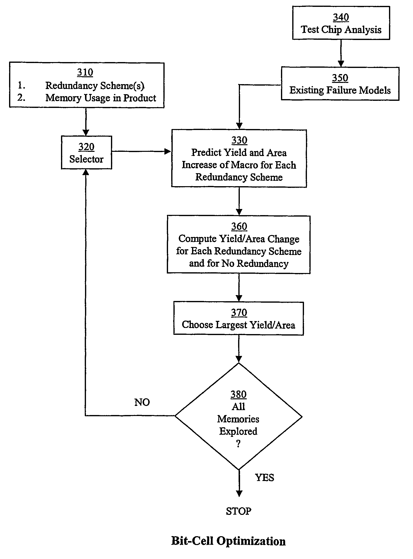
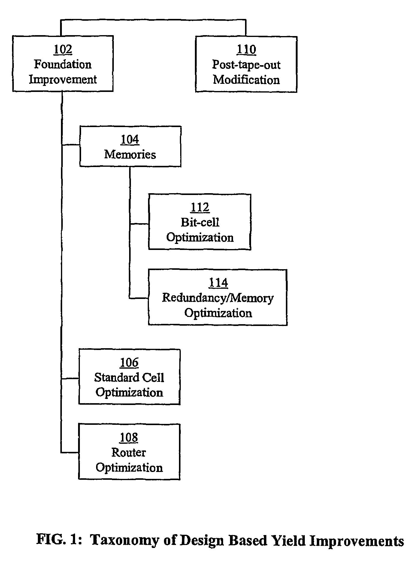
[0027]FIG. 1 shows an exemplary taxonomy of yield estimation and improvement process components. Foundation improvements 102 include changes that are made to libraries, memories, or other elements that are common to many designs. Post-tape-out modifications 110 are changes that are made after a design has been completed. Within foundation improvements 102, one can generally classify improvements into three categories: memories 104, standard cells 106, and routers 108. Memories 104 can further be classified into changes to bit-cells 112 and redundancy / memory optimization changes 114.

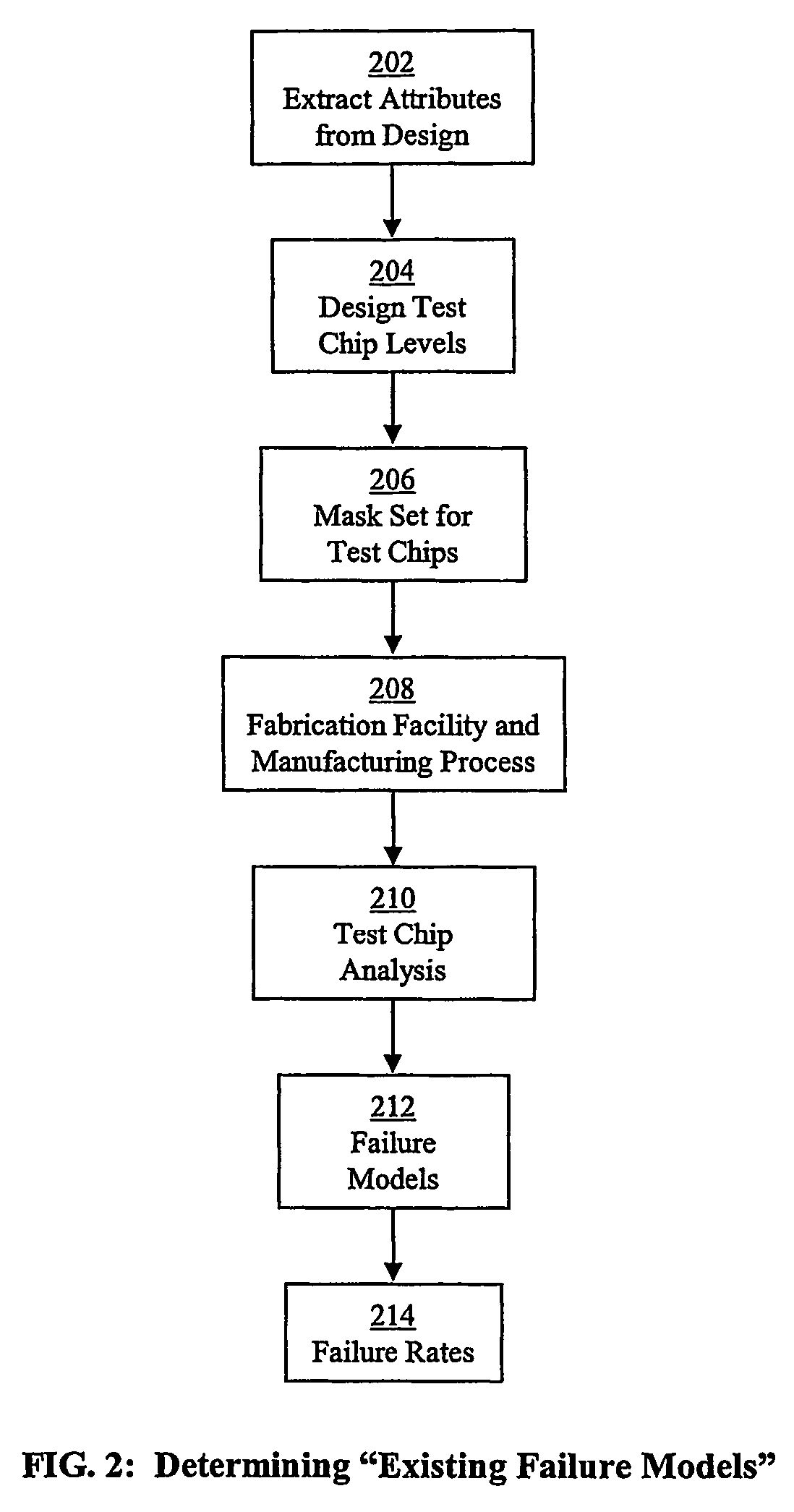
[0028]2. Test Chip Analysis

[0029]FIG. 2 illustrates an exemplary method for obtaining the fa...


PUM


Abstract

An integrated circuit is designed to improve yield when manufacturing the integrated circuit, by obtaining a design element from a set of design elements used in designing integrated circuits. A variant design element is created based on the obtained design element, where a feature of the obtained design element is modified to create the variant design element. A yield to area ratio for the variant design element is determined. If the yield to area ratio of the variant design element is greater than a yield to area ratio of the obtained design element, the variant design element is retained to be used in designing the integrated circuit.

Description

CROSS REFERENCE TO RELATED APPLICATION[0001]This application is a National Stage of International Application No. PCT / US03 / 037046, filed Nov. 17, 2003, and claims the benefit of an earlier filed provisional application U.S. Provisional Application Ser. No. 60 / 437,922, entitled YIELD IMPROVEMENT, filed on Jan. 2, 2003, the entire content of which is incorporated herein by reference.BACKGROUND[0002]1. Field of the Invention[0003]The present application relates to chip design and, in particular, to optimizing existing design rules for improving semiconductor chip fabrication yield.[0004]2. Related Art[0005]The fabrication of integrated circuits is an extremely complex manufacturing process that may involve hundreds of individual operations. Basically, the process includes the diffusion of precisely determined amounts of dopant material into precisely determined areas of a silicon wafer to produce active devices such as transistors. This is typically accomplished by forming a layer of s...

Claims


Application Information

Patent Timeline
Patent Type & Authority Patents(United States)
IPC IPC(8): G06F17/50H01L
CPCG06F17/5045G06F30/30
Inventor CIPLICKAS, DENNISDAVIS, JOEHESS, CHRISTOPHERLEE, SHERRYMALAVASI, ENRICOMOHAMMAD, ABDULMOBEENRADOJCIC, RATIBORSTINE, BRIANVALLISHAYEE, RAKESHZANELLA, STEFANODRAGONE, NICOLAGUARDIANI, CARLOQUARANTELLI, MICHELTONELLO, STEFANOANIRUDDHA, JOSHI
Owner PDF SOLUTIONS INC
Why Eureka
Try Eureka