Radiation image detector

a detector and radiation image technology, applied in the direction of instruments, radiation controlled devices, optical radiation measurement, etc., can solve the problems of increasing production costs, not practicable, and the pixel size is limited to around 100 m squar

Inactive Publication Date: 2009-02-10
FUJIFILM CORP
View PDF8 Cites 4 Cited by
  • Summary
  • Abstract
  • Description
  • Claims
  • Application Information

AI Technical Summary

Benefits of technology

[0028]The radiation image detector of the present invention includes the following layers stacked on top of another: a charge generation layer that generates charges by receiving radiation; and a detection layer including: multitudes of pixels, each having a collection electrode for collecting charges generated in the charge generation layer, a storage capacitor for storing charges collected by the collection electrode, and a TFT switch for reading out charges stored in the storage capacitor; multitudes of scanning lines for switching ON / OFF the TFT switches; and multitudes of data lines through which charges stored in the storage capacitors are read out. Here, each of the storage capacitors is formed between a storage capacitor electrode connected to the drain electrode of a TFT switch and the scanning line connected to a TFT switch adjacent to the TFT switch to which the drain electrode belongs, an array of the TFT switches is divided into upper and lower halves for driving, each of the data lines is divided into upper and lower halves, and a dummy wire is provided at the division boundary section of the upper and lower halves of the array of the TFT switches for forming a storage capacitor of a pixel disposed at the division boundary section. This arrangement allows the storage capacitors to be provided for the pixels at the division boundary section, thereby a step difference in the image at the division boundary section may be made less noticeable.
[0029]Further, if the radiation image detector of the present invention include a TFT switch drive section for performing detection on the array of the TFT switches from upper and lower ends of the array, variations in the potential of the charges stored in the storage capacitors may be prevented, and noise in detected image data may be reduced.
[0031]Further, if the dummy wires, each provided for each row of pixels located on each of the upper and lower sides of the division boundary section, are disposed at such a distance that the collection electrodes are disposed at equally spaced apart in the up / down directions, the spacing of the collection electrodes becomes uniform, thereby a step difference in the image at the division boundary section may be made less noticeable.
[0032]Still further, if the collection electrode of each pixel of each pixel row located on each of the upper and lower sides of the division boundary section is disposed such that the distance between the collection electrode of the pixel of the pixel row on the upper side of the division boundary section and the collection electrode of the corresponding pixel of the pixel row on the lower side of the division boundary becomes close to the distance between the collection electrodes of the pixels other than the pixels of the pixel rows in the up / down directions, the spacing of the collection electrodes becomes close to uniform, thereby a step difference in the image at the division boundary section may be made less noticeable.

Problems solved by technology

The pixel size, however, is practically limited to around 100 μm square due to restrictions arising from the TFT array structure.
This is not practical because of a significant increase in the production cost.
As a result, the electrical noise has also increased.

Method used


Image

  • Radiation image detector
  • Radiation image detector
  • Radiation image detector

Examples


first embodiment

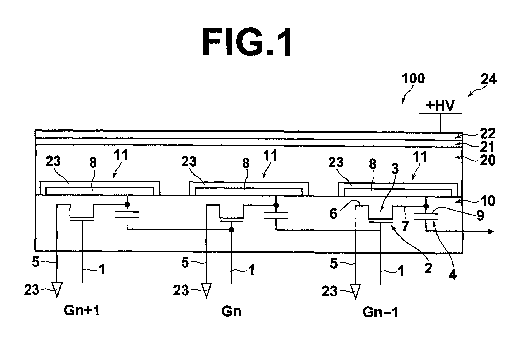
[0046]Hereinafter, the radiation image detector of the present invention will be described with reference to the accompanying drawings.

[0047]A flat panel image sensor, as the radiation image detector of the present embodiment, is an image sensor capable of detecting an image represented by X-rays or the like, and is used, for example, in X-ray imaging equipment that creates a picture of an X-ray image transmitted through a human body or the like. It is noted that the radiation image detector of the present invention is not necessarily limited to the flat panel type, and includes an image sensor with a curved surface substrate.

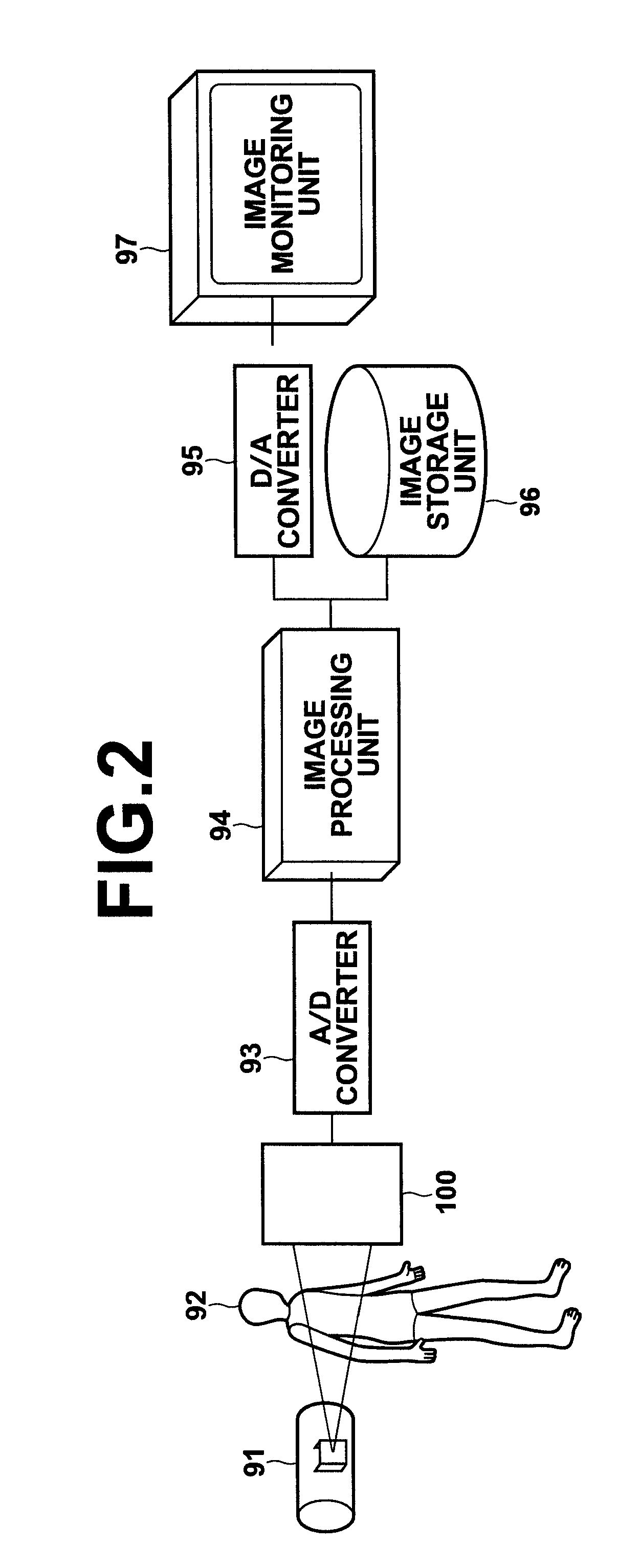
[0048]That is, for example, an X-ray transmission image of a subject 92 formed by X-rays outputted from an X-ray tube 91 is converted to image signals by a radiation image detector 100 of the present embodiment, in which photoelectric conversion elements are disposed in a two dimensional array, as illustrated in FIG. 2.

[0049]Analog image signals outputted from ...

third embodiment

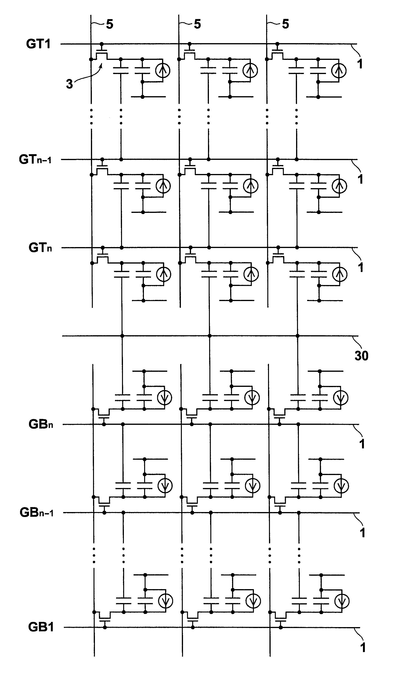
[0075]In the radiation image detector the dummy wires 30a, 30b are disposed such that the distance Wd between them is smaller than the distance Ws between the scanning lines. That is, they are disposed at such a distance that the collection electrodes 8 are disposed at equally spaced apart in the up / down directions.

[0076]By disposing the dummy wires 30a, 30b in the manner as described above, a visual step difference in the image due to space misalignment of the collection electrodes 8 may be reduced.

[0077]Next, the radiation image detector according to a fourth embodiment of the present invention will be described. The radiation image detector according to the present embodiment is identical in general configuration to the radiation image detector according to the second embodiment, but differs in the method of disposing the collection electrodes 8 of the pixels 11 at the division boundary section. A layout of the radiation image detector according to the fourth embodiment is illus...


PUM


Abstract

A radiation image detector including a charge generation layer, and a detection layer including: many pixels, each having a collection electrode for collecting charges generated in the charge generation layer, a storage capacitor for storing charges collected by the collection electrode, and a TFT switch for reading out charges from the storage capacitor; many scanning lines; and many data lines. Each storage capacitor is formed between a storage capacitor electrode connected to the drain electrode of a TFT switch and the scanning line connected to a TFT switch adjacent to the TFT switch to which the drain electrode belongs, an array of the TFT switches is divided into upper and lower halves, each data line is divided into upper and lower halves, and a dummy wire is provided at the division boundary for forming a storage capacitor of a pixel disposed at the division boundary section.

Description

BACKGROUND OF THE INVENTION[0001]1. Field of the Invention[0002]The present invention relates to a radiation image detector which includes the following layers stacked on top of another: a charge generation layer that generates charges by receiving radiation; and a detection layer in which multitudes of pixels, each having a TFT switch, are disposed two dimensionally.[0003]2. Description of the Related Art[0004]Recently, flat panel detectors (FPDs) have been put into practical use. FPD includes an X-ray sensitive layer on a TFT active matrix array and is capable of directly converting X-ray information to digital data. It has advantages over conventional imaging plates in that it allows instantaneous image verification and checking for motion images, and is spreading rapidly.[0005]First, the configuration of a conventional radiation image detector will be described with reference to FIG. 10.[0006]In the conventional radiation image detector, a semiconductor layer 20 which is conduct...

Claims


Application Information

Patent Timeline
Patent Type & Authority Patents(United States)
IPC IPC(8): G01T1/24
CPCG01T1/2928G01T1/247
Inventor OKADA, YOSHIHIRO
Owner FUJIFILM CORP
Why Eureka
Try Eureka