
Method for achieving uniform etch depth using ion implantation and a timed etch

a technology of ion implantation and uniform etch depth, which is applied in the direction of basic electric elements, electrical equipment, semiconductor devices, etc., can solve the problems of significant device and circuit performance variation, inconvenient etching, and inability to achieve uniform etch depth, etc., to achieve the effect of enhancing the etch rate of silicon dioxide, and enhancing the etch ra

Active Publication Date: 2009-02-24
SYNOPSYS INC
View PDF3 Cites 1 Cited by
  • Summary
  • Abstract
  • Description
  • Claims
  • Application Information

AI Technical Summary

Benefits of technology

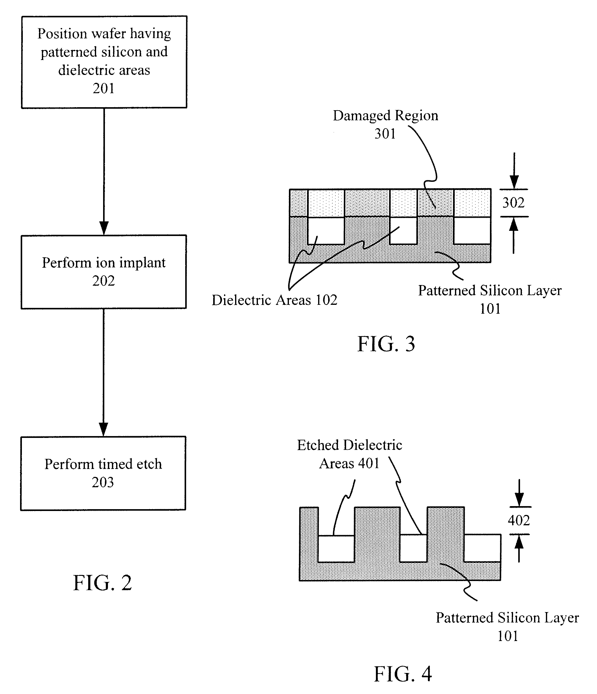
[0007]A method of performing a timed etch of a material to a precise depth is provided. In this method, ion implantation of the material is performed before the timed etch. This ion implantation process substantially enhances the etch rate of the material within a precisely controlled depth range corresponding to the range of implantation-induced damage. That is, the damaged material etches significantly faster than the undamaged material. Note that the range of the implantation-induced damage can be tailored by adjusting the implanted ion species, dose, and energy. Generally, the larger the ion mass, the lower the dose required to induce a threshold level of damage required to enhance the etch rate. For example, if argon (Ar) is the implanted ion species, a dose of 1E14 per square centimeter can adequate to significantly enhance the etch rate of silicon dioxide. The depth to which a threshold level of damage is achieved increases approximately logarithmically with the implanted dose, whereas it increases linearly with the projected ion range that is determined by the implant energy.
[0008]Advantageously, by performing the ion implantation prior to etching, the variation in vertical etch depth can be reduced by a factor approximately equal to the etch rate of the damaged material divided by the etch rate of the undamaged material. The vertical etch depth can be used to provide a vertical dimension of a non-planar semiconductor device. Minimizing vertical device dimension variations on a wafer can reduce device and circuit performance variations, which is highly desirable.

Problems solved by technology

Unfortunately, the etch rate across a wafer is typically not perfectly uniform due to equipment imperfections, variations in IC pattern density, and / or inherent conditions associated with the etch process being used.
In turn, these vertical device dimension variations may result in significant device and circuit performance variations, which is highly undesirable.

Method used


Image

  • Method for achieving uniform etch depth using ion implantation and a timed etch
  • Method for achieving uniform etch depth using ion implantation and a timed etch
  • Method for achieving uniform etch depth using ion implantation and a timed etch

Examples


Embodiment Construction

[0017]In accordance with one aspect of the invention, ion implantation can be used to improve the uniformity and controllability of a timed etch. As described below, this ion implantation can advantageously enhance the etch rate within a depth range that reaches down to a desired etch depth.

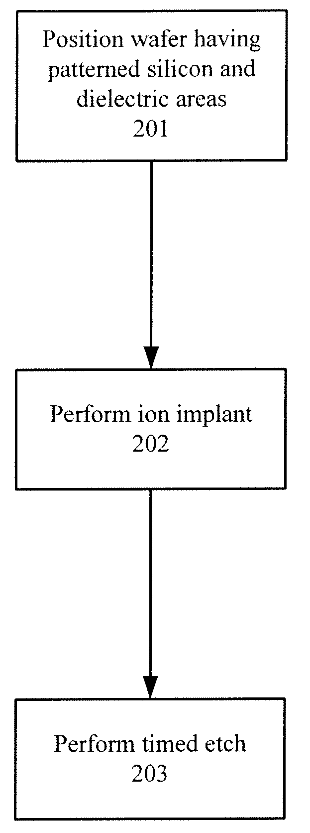
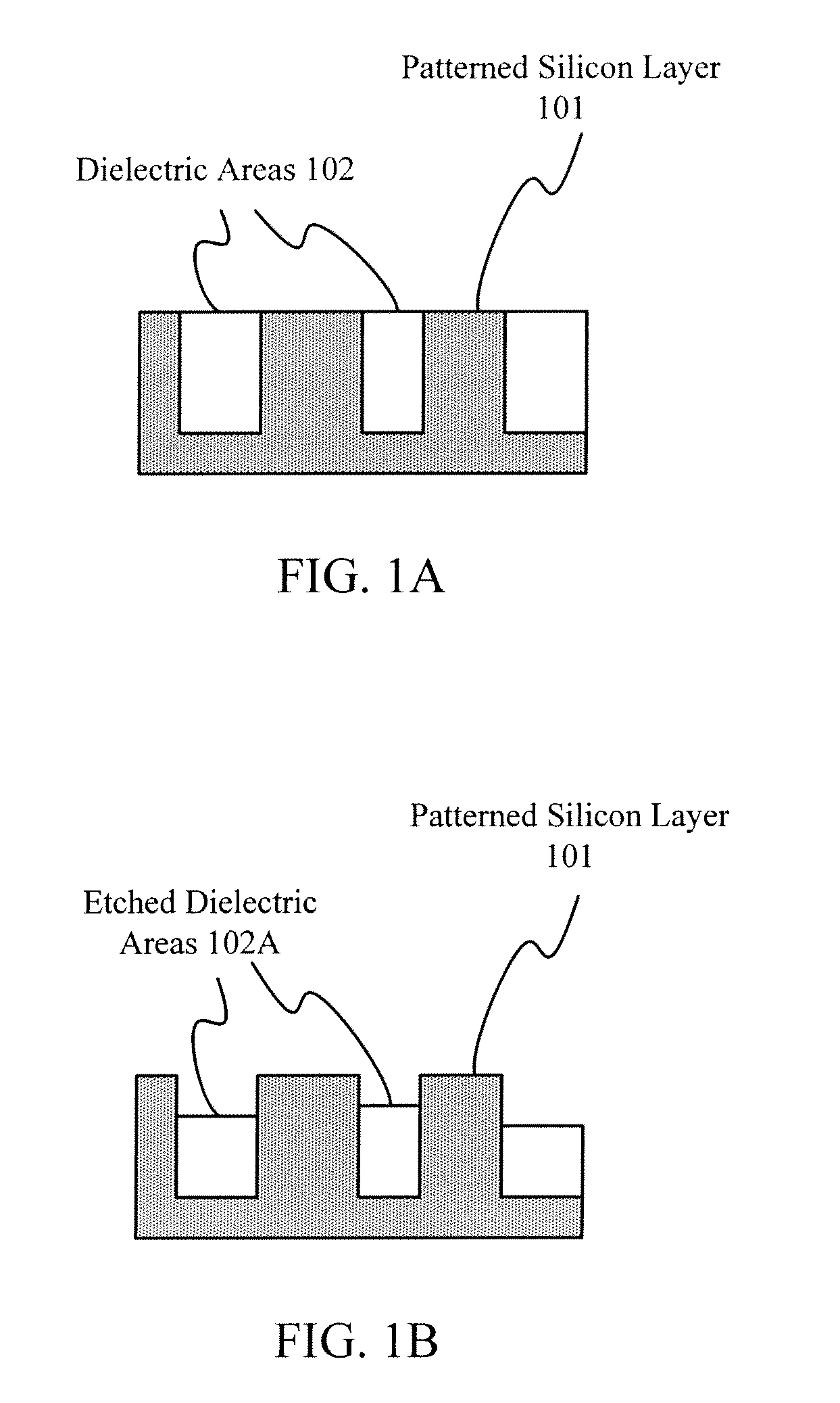
[0018]FIG. 2 illustrates exemplary steps for improving the uniformity and controllability of a timed etch. In step 201, a wafer having patterned silicon and dielectric areas can be positioned for an etching process. This wafer could have a simplified cross-section similar to that shown in FIG. 1A.

[0019]In step 202, an ion implantation process can be performed. The implantation effectively “damages” the upper portions of the silicon and dielectric areas. In other words, much like spraying a plaster wall with bullets can facilitate the subsequent removal of the plaster, ion implantation can accelerate the subsequent removal of the implanted material during a subsequent timed etch. As shown in FIG. ...


PUM


Abstract

A method of performing a timed etch of a material to a precise depth is provided. In this method, ion implantation of the material is performed before the timed etch. This ion implantation process substantially enhances the etch rate of the material within a precisely controlled depth range corresponding to the range of implantation-induced damage. By using the ion implantation, the variation in vertical etch depth can be reduced by a factor approximately equal to the etch rate of the damaged material divided by the etch rate of the undamaged material. The vertical etch depth can be used to provide a vertical dimension of a non-planar semiconductor device. Minimizing vertical device dimension variations on a wafer can reduce device and circuit performance variations, which is highly desirable.

Description

BACKGROUND OF THE INVENTION[0001]1. Field of the Invention[0002]The present invention relates to the field of semiconductor integrated-circuit (IC) manufacturing, and in particular a technique of providing uniform etch depth by using ion implantation and a timed etch.[0003]2. Description of the Related Art[0004]The vertical dimensions of semiconductor devices (e.g. capacitors, transistors) with non-planar surfaces are often defined simply by a timed etch of a homogeneous dielectric (e.g. oxide) material that serves to electrically isolate semiconductor device regions. For example, FIG. 1A illustrates a cross-sectional view of a patterned silicon layer 101 and dielectric areas 102 that can provide electrical isolation. During the process of forming devices in patterned silicon layer 101, dielectric areas 102 can be etched. Generally, this etch has high selectivity between materials, thereby etching dielectric areas 102 much more quickly than patterned silicon layer 101. In some embod...

Claims


Application Information

Patent Timeline
Patent Type & Authority Patents(United States)
IPC IPC(8): H01L21/302
CPCH01L21/31111H01L21/31116H01L21/32133H01L21/26506H01L29/66795H01L29/7853H10B12/36H10B12/056H01L21/3105H01L21/324H01L21/76224H01L29/0653H01L29/785
Inventor LIU, TSU-JAE KING
Owner SYNOPSYS INC
Learn More