

Method of configuring superconducting random access memory, device structure of the same, and superconducting drive circuit
a superconducting random access and drive circuit technology, applied in the direction of digital storage, instruments, code conversion, etc., can solve the problems of large power consumption and high-speed operation problems, increase operating time, and difficulty in achieving two-direction consistency logic. , to achieve the effect of high-load drive capability, high-speed operation and a large reduction of power consumption
- Summary
- Abstract
- Description
- Claims
- Application Information
AI Technical Summary
Benefits of technology
Problems solved by technology
Method used
Image

Examples
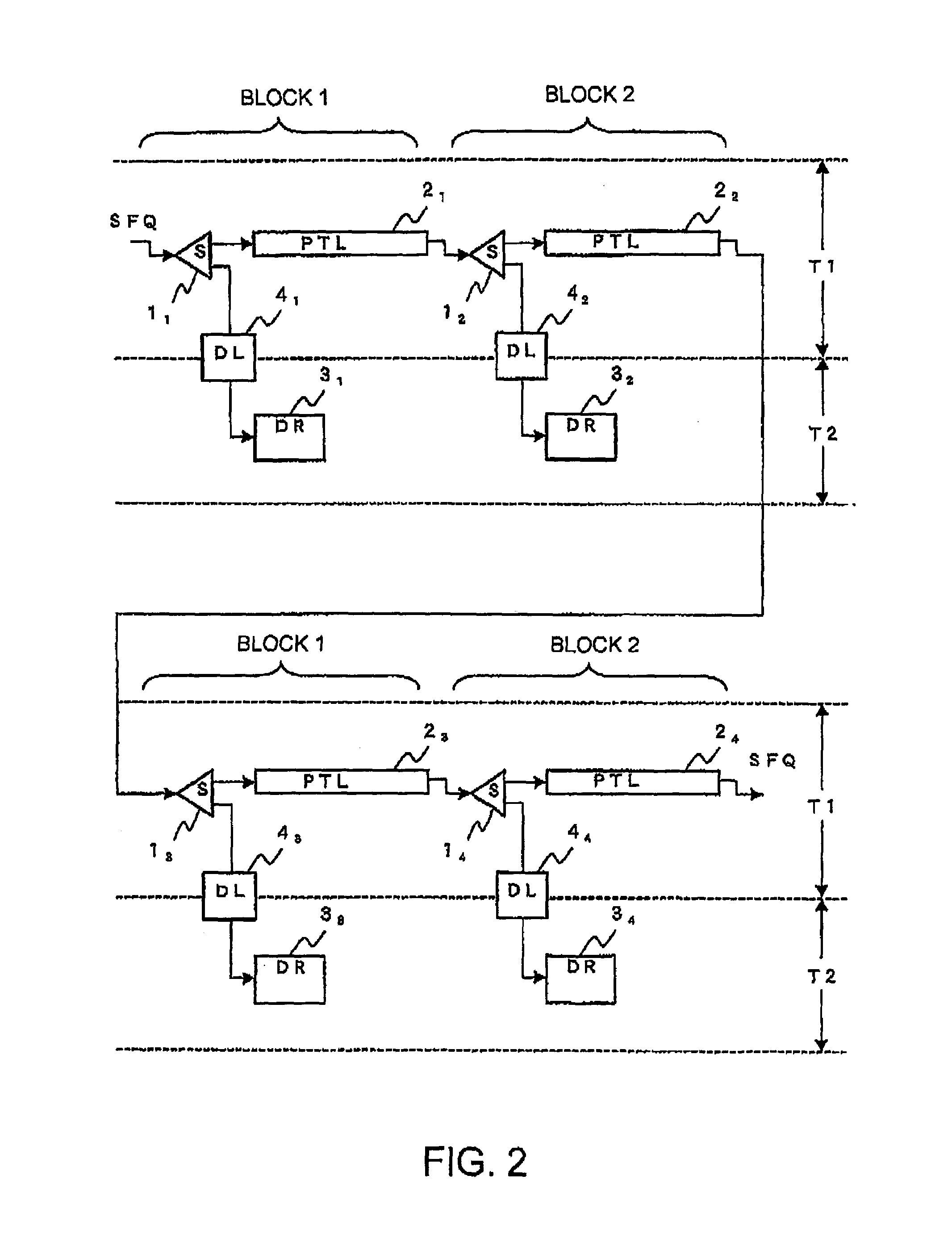
sixth embodiment
[0181]Referring to FIG. 6, description will be made about a sixth embodiment of this invention.
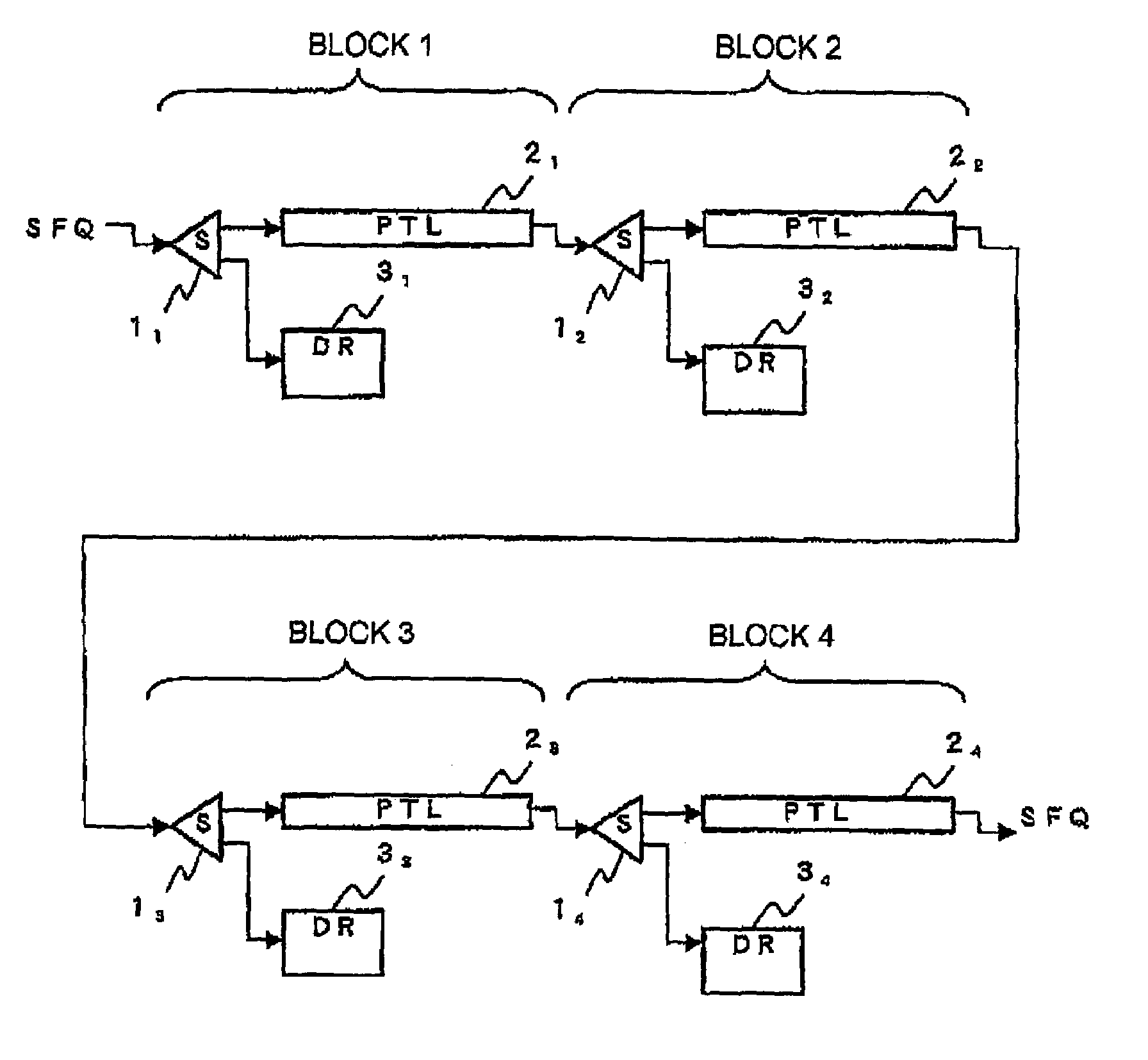
[0182]FIG. 6 is an equivalent circuit diagram showing the structure of a superconducting RAM according to the sixth embodiment of this invention. The sixth embodiment is a first example relating to the structure of a sense line in the superconducting RAM.
[0183]At first, the structure and function of this circuit will be described.
[0184]The sixth embodiment comprises in-block signal propagation circuits (DR) 61 to 64, superconducting passive transmission lines (PTL)21 to 24 adapted to carry out signal propagation between blocks, and confluence buffers (C) 71 to 74 each formed by a single flux quantum (SFQ) device and each adapted to receive a signal from a corresponding one of the superconducting passive transmission lines (PTL) 21 to 24 or a corresponding one of the in-block signal propagation circuits (DR) 61 to 64 and propagate it to the superconducting passive transmission line (PTL) of...
seventh embodiment
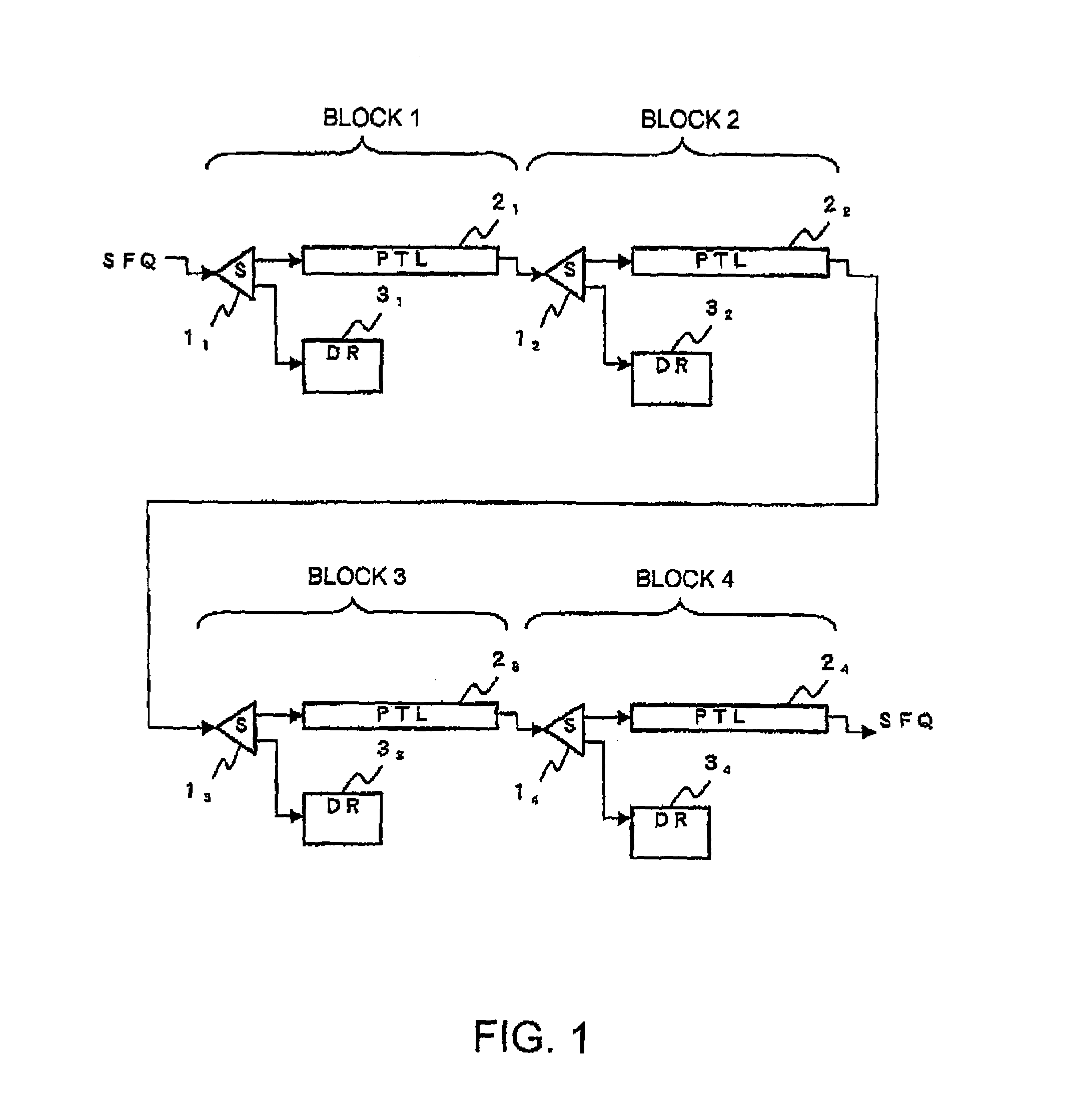
[0189]Referring to FIG. 7, description will be made about a seventh embodiment of this invention.
[0190]FIG. 7 is an equivalent circuit diagram showing the structure of a superconducting RAM according to the seventh embodiment of this invention. The seventh embodiment is a second example relating to the structure of a sense line in the superconducting RAM.
[0191]At first, the structure and function of the circuit according to the seventh embodiment will be described.
[0192]The seventh embodiment comprises in-block signal propagation circuits (DR) 61 to 64, superconducting passive transmission lines (PTL) 21 to 24 adapted to carry out signal propagation between blocks, latch circuits (DL) 41 to 44 each formed by a single flux quantum (SFQ) device and each having a function of holding information, and confluence buffers (C) 71 to 74 each formed by a single flux quantum (SFQ) device and each adapted to receive a signal from a corresponding one of the superconducting passive transmission l...
eighth embodiment
[0197]Referring to FIG. 8, description will be made about an eighth embodiment of this invention.
[0198]FIG. 8 is an equivalent circuit diagram showing the structure of a superconducting RAM according to the eighth embodiment of this invention. The eighth embodiment is a third example relating to the structure of a sense line in the superconducting RAM.
[0199]At first, the structure and function of the circuit according to the eighth embodiment will be described.
[0200]The eighth embodiment is configured such that the interblock signal propagation circuit formed by the passive transmission lines (PTL) and the confluence buffers (C) in the seventh embodiment is arranged in a binary tree. In addition, this embodiment is set to operate in a three-stage pipeline by inserting latch circuits (DL) at proper positions in the interblock signal propagation circuit of the binary tree structure.
[0201]Now, description will be made about the structure of the eighth embodiment including a portion omi...
PUM
 Abstract
Description
Claims
Application Information