Method for manufacturing display device with conductive resonator spacer layers having different total thicknesses

a technology of conductive resonator and spacer layer, which is applied in the manufacture of electric discharge tubes/lamps, cold cathode manufacturing, and electromechanical systems, etc. it can solve the problems of insufficient light emission brightness of currently proposed organic el elements, inability to actually employ a display device, and acceleration of deterioration of organic layers, so as to achieve easy and accurate formation of optical microresonators, easy to change, and high positional precision

Active Publication Date: 2009-03-31
SANYO ELECTRIC CO LTD
View PDF29 Cites 27 Cited by
  • Summary
  • Abstract
  • Description
  • Claims
  • Application Information

AI Technical Summary

Benefits of technology

[0026]According to the present invention, it is possible to easily and accurately form an optical microresonator for each light emission wavelength (intensification wavelength) in each pixel of a display device. In particular, the conductive resonator spacer layer can be formed with a high positional precision through photolithography. In addition, a total thickness of the conductive resonator spacer layer can be easily changed corresponding to the light emission wavelengths by forming the conductive resonator spacer layer while changing the number of layers or a number of remaining layers of a plurality of, for example, conductive metal oxide layers.
[0027]Regarding the number of layers or the number of remaining layers of the conductive metal oxide layers, it is possible to easily change these numbers with a high thickness precision by taking advantage of a difference in the etching rates of the amorphous conductive metal oxide and the polycrystalline conductive metal oxide and selectively removing the amorphous conductive metal oxide layer formed in an upper layer using the polycrystalline conductive metal oxide layer formed in a lower layer as the etching stopper.

Problems solved by technology

However, the light emission brightness of currently proposed organic EL elements is not sufficient.
In addition, there is a problem in that, when the supplied current to the organic layer is increased in order to improve the light emission brightness, deterioration of the organic layer is accelerated.
Therefore, no structure can be actually employed as a display device unless the structure can stably achieve a high display quality in all pixels.
Because of this, although, for example, theoretically, the cavity (resonator) structure as described above can be realized in a full color display device by setting the optical length in each pixel depending on the light emission wavelength, when the pixels are independently manufactured to achieve different thicknesses, the number of processes in the manufacturing is inevitably increased and the manufacturing processes become more complicated, which results in serious degradation of the quality and variation.
In particular, because an organic EL display device currently has a problem with respect to the stability of the display quality, if a resonator structure is simply used, the yield is reduced when the display devices are mass-produced and the manufacturing cost is significantly increased.
Therefore, application of the microresonator to an EL display device has been only researched and has not yet been commercialized.

Method used


Image

  • Method for manufacturing display device with conductive resonator spacer layers having different total thicknesses
  • Method for manufacturing display device with conductive resonator spacer layers having different total thicknesses
  • Method for manufacturing display device with conductive resonator spacer layers having different total thicknesses

Examples


Embodiment Construction

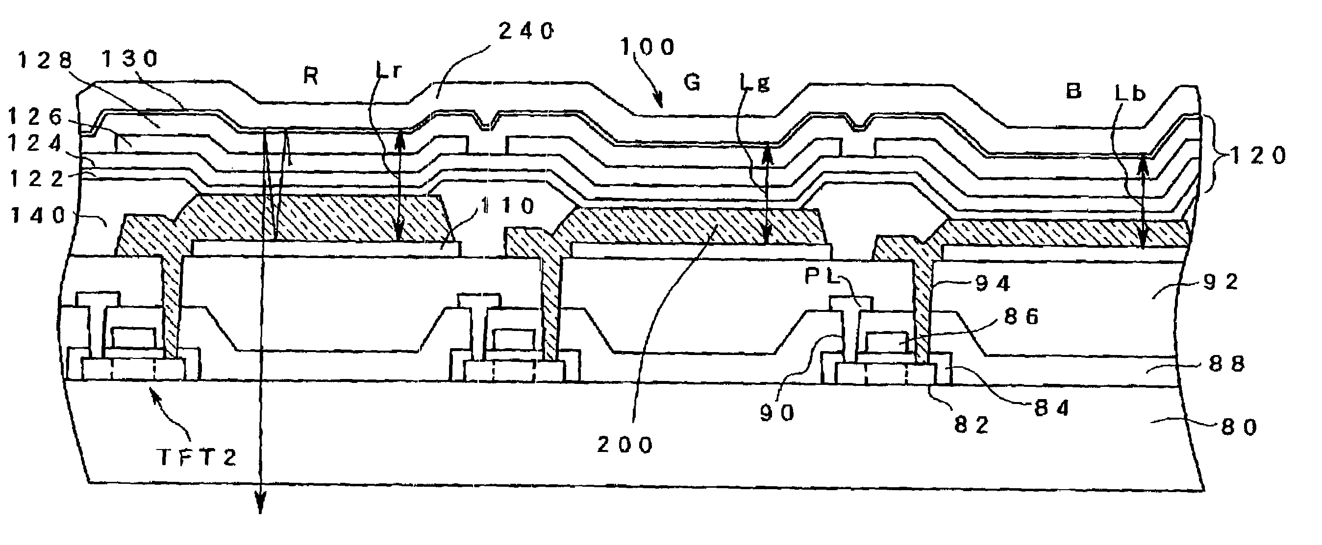
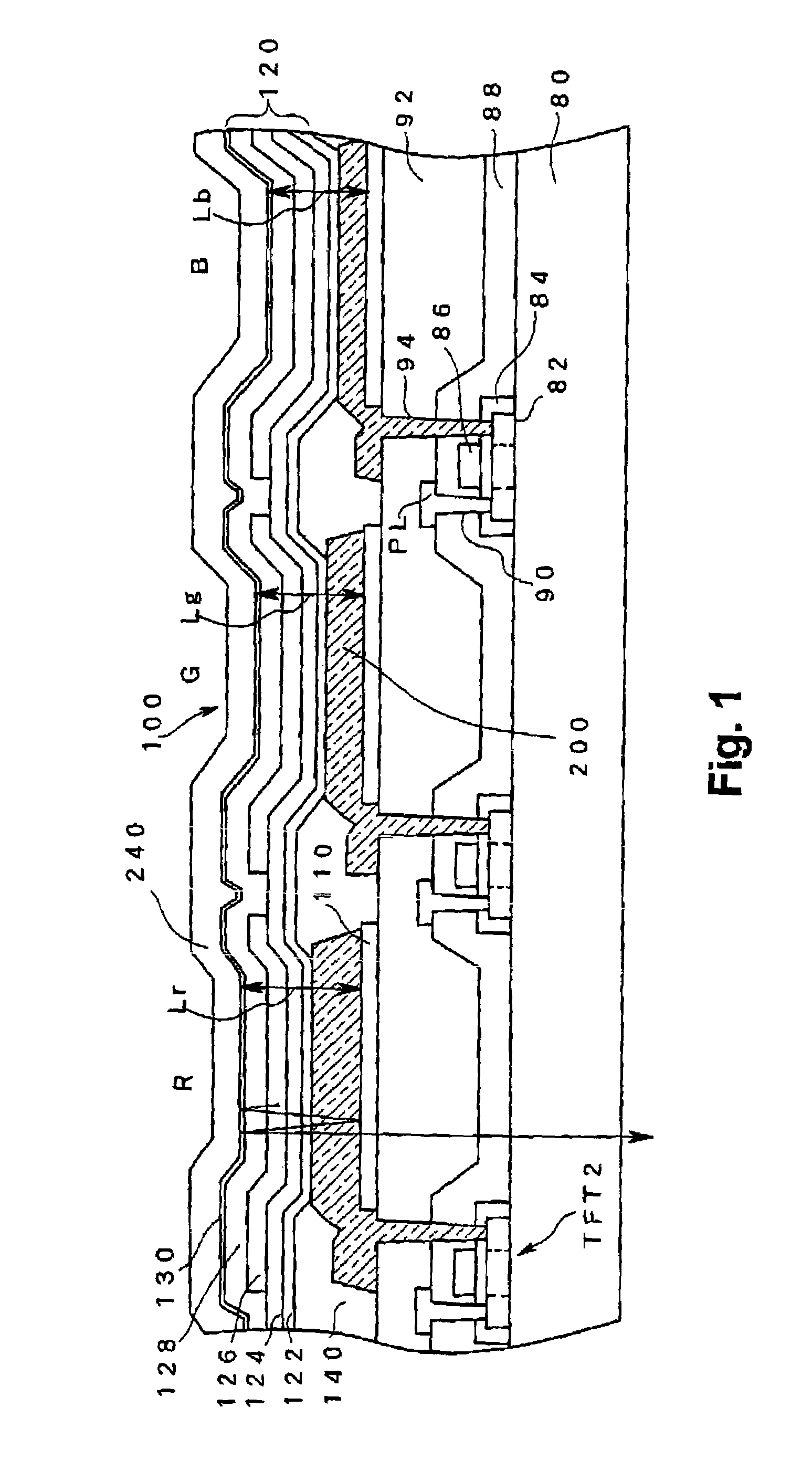
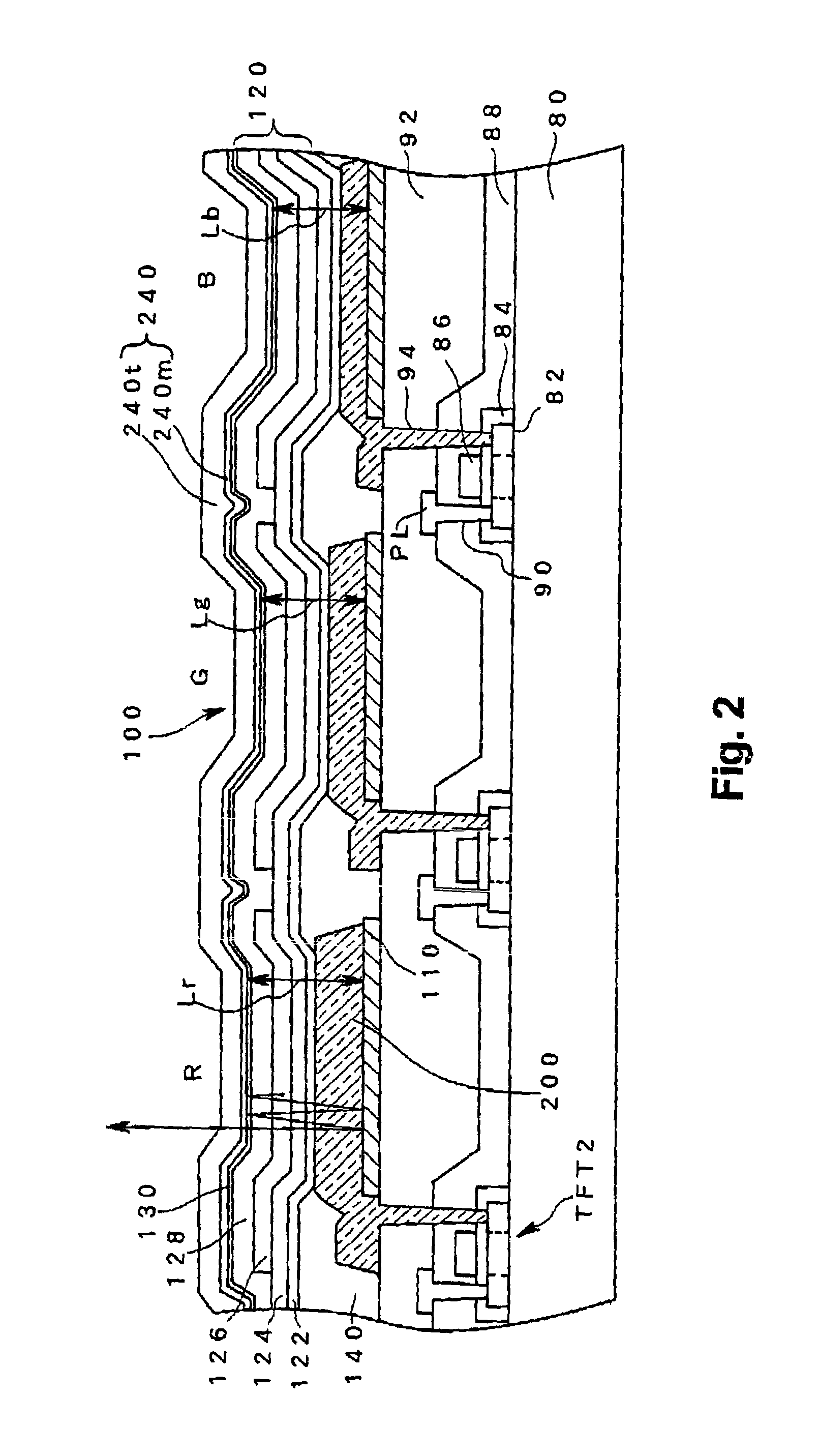
[0037]A preferred embodiment (hereinafter, referred to simply as “embodiment”) of the present invention will now be described referring to the drawings.

[0038]FIG. 1 is a diagram schematically showing a cross sectional structure of a display device having a microresonator (microcavity) structure according to a preferred embodiment of the present invention. The display device is a light emitting display device having a self-emissive display element in each pixel. The present invention will be described exemplifying an organic EL display device in which an organic EL element is used as the display element.

[0039]An organic EL element 100 has a layered structure having an organic light emitting element layer 120 which at least includes an organic compound, in particular, an organic light emitting material, between a first electrode 200 and a second electrode 240. The organic EL element 100 takes advantage of a principle that electrons are injected from an anode to the organic layer and h...


PUM


Abstract

A display device having a plurality of pixels and which realizes a color display with emitted light of at least two wavelengths wherein each pixel has a microresonator structure between a lower reflective film formed on a side near a substrate and an upper reflective film formed above the lower reflective film with an organic light emitting element layer therebetween. The lower reflective film is made of a metal thin film and a conductive resonator spacer layer which functions as a first electrode is provided between the lower reflective film and the organic light emitting element layer. A thickness of the conductive resonator spacer layer is changed by changing a number of layers or a number of remaining layers of transparent conductive metal oxide layers made of ITO corresponding to pixels of different light emission wavelengths. An amorphous ITO layer at an upper layer is selectively removed from above a polycrystalline ITO layer at a lower layer using the polycrystalline ITO layer as an etching stopper so that the thickness is changed corresponding to the thickness of the ITO layer to be formed and not removed. Light obtained in the organic light emitting element layer is intensified by the microresonator structure in which the optical length is adjusted by the conductive resonator spacer layer and is emitted to the outside.

Description

CROSS-REFERENCE TO RELATED APPLICATIONS[0001]The entire disclosure of Japanese Patent Application No. 2003-435821 including specification, claims, drawings and abstract is incorporated herein by reference.BACKGROUND OF THE INVENTION[0002]1. Field of the Invention[0003]The present invention relates to a display device and, in particular, to a color display device having a microresonator (microcavity) structure.[0004]2. Description of the Related Art[0005]In recent years, flat panel displays (FPD) having a thin thickness and which allow reduction in size have attracted much attention. Of various FPDs, liquid crystal display devices are used in various devices. Currently, there is intense research and development into light emitting devices (display devices and light sources) in which a self-emitting electroluminescence (hereinafter referred to simply as “EL”) elements, in particular, organic EL display devices which can emit light at various light emission colors and at a high brightn...

Claims


Application Information

Patent Timeline
Patent Type & Authority Patents(United States)
IPC IPC(8): H01J9/00H05B33/10H01J9/24H01L27/32H01L51/50H01L51/52H05B33/12H05B33/14H05B33/22H05B33/24
CPCH01L27/3211H01L51/5265H01L51/5203H10K59/35H10K50/852H10K59/805H05B33/10H05B33/22H10K50/805
Inventor SUZUKI, KOJI
Owner SANYO ELECTRIC CO LTD
Why Eureka
Try Eureka