Semiconductor integrated device for preventing breakdown and degradation of a gate oxide film caused by charge-up in manufacturing steps thereof, design method thereof, designing apparatus method thereof, and maunfacturing apparatus thereof

a technology of integrated devices and semiconductors, applied in the direction of semiconductor/solid-state device details, instruments, computer aided design, etc., can solve the problems of inability to achieve a sufficiently stable semiconductor integrated circuit with respect to the antenna, the influence of parasitic capacitance between wirings will increase, and the effect of reducing the size of the chip cannot be achieved

Inactive Publication Date: 2009-04-21
RENESAS ELECTRONICS CORP
View PDF14 Cites 12 Cited by
  • Summary
  • Abstract
  • Description
  • Claims
  • Application Information

AI Technical Summary

Benefits of technology

[0034]According to the present invention, as a measure against an antenna effect, the semiconductor integrated device is designed and manufactured also in consideration of an influence caused by charge-up on the wiring or the like adjacent to the wiring connected to the gate. Accordingly, even if smaller device geometries is pursued in a semiconductor process, the high-quality semiconductor integrated device having wirings with the proper measure against the antenna effect taken therein and without device degradation can be obtained.

Problems solved by technology

As smaller device geometries are achieved in a semiconductor process, however, the influence of parasitic capacitance between wirings will increase.
Thus, it has become difficult to obtain the semiconductor integrated circuit that is sufficiently stable with respect to the antenna effect.
Accordingly, it has more often occurred that sufficient reduction in the size of a chip cannot be achieved.

Method used


Image

  • Semiconductor integrated device for preventing breakdown and degradation of a gate oxide film caused by charge-up in manufacturing steps thereof, design method thereof, designing apparatus method thereof, and maunfacturing apparatus thereof
  • Semiconductor integrated device for preventing breakdown and degradation of a gate oxide film caused by charge-up in manufacturing steps thereof, design method thereof, designing apparatus method thereof, and maunfacturing apparatus thereof
  • Semiconductor integrated device for preventing breakdown and degradation of a gate oxide film caused by charge-up in manufacturing steps thereof, design method thereof, designing apparatus method thereof, and maunfacturing apparatus thereof

Examples


first embodiment

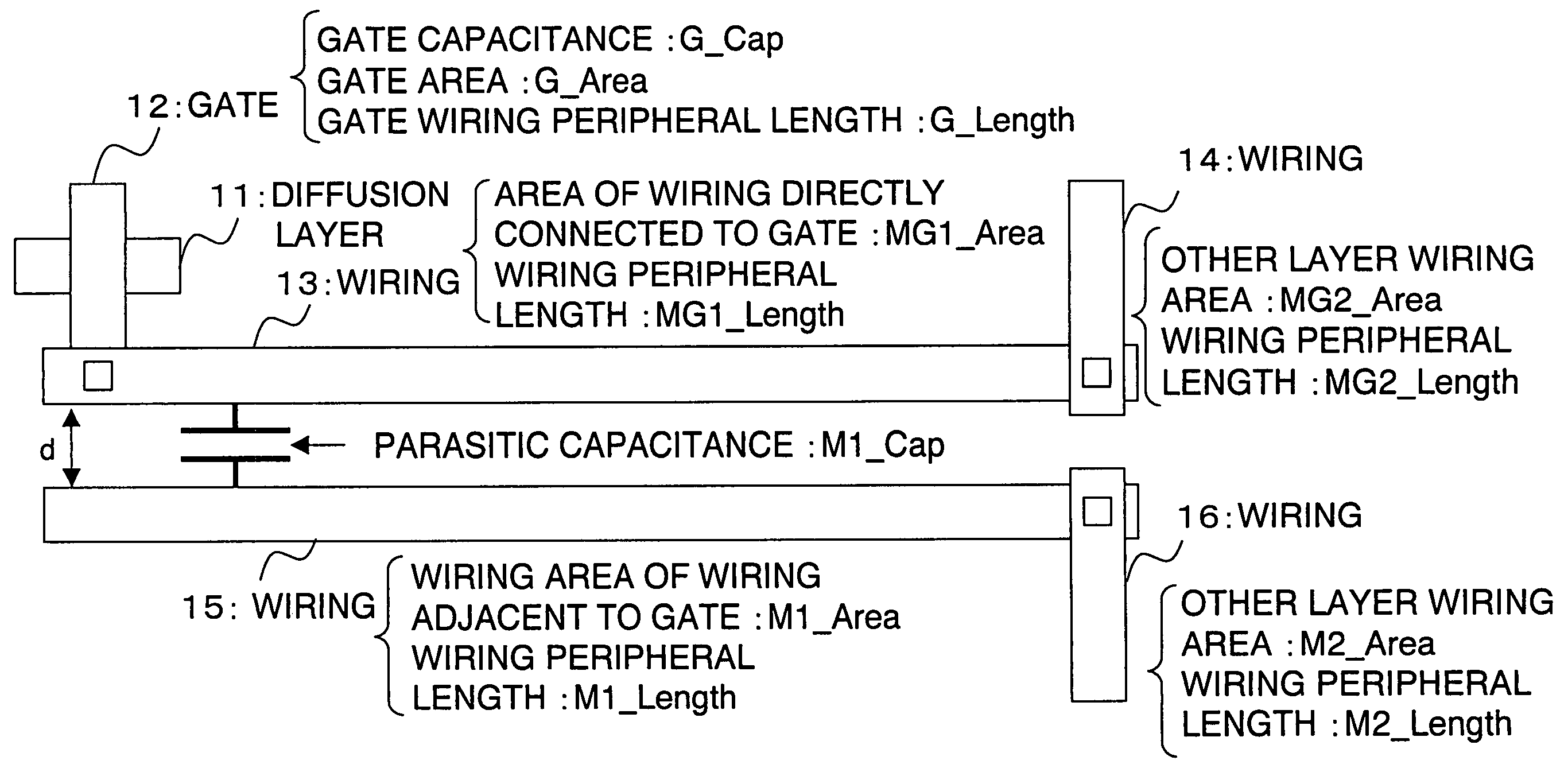
[0049]FIG. 1 is a diagram showing a layout of a semiconductor integrated circuit according to a first embodiment of the present invention. Referring to FIG. 1, a gate 12 is arranged insulated from the diffusion layer 11 of the transistor. A wiring 13 is directly wired to the gate 12, and a wiring 14 connected to the wiring 13 is wired in other layer. A wiring 15 is arranged in parallel with the wiring 13 with a spacing d provided therebetween. Further, a wiring 16 connected to the wiring 15 is wired in other layer.

[0050]Herein, the gate area of the gate 12 is indicated by G_Area, the gate capacitance of the gate 12 is indicated by G_Cap, the peripheral length of the gate wiring of the gate 12 is indicated by G_Length. The area of the wiring 13 is indicated by MG1_Area, and the wiring peripheral length of the wiring 13 is indicated by MG1_Length. The area of the wiring 14 is indicated by MG2_Area, and the wiring peripheral length of the wiring 14 is indicated by MG2_Length. The area ...

second embodiment

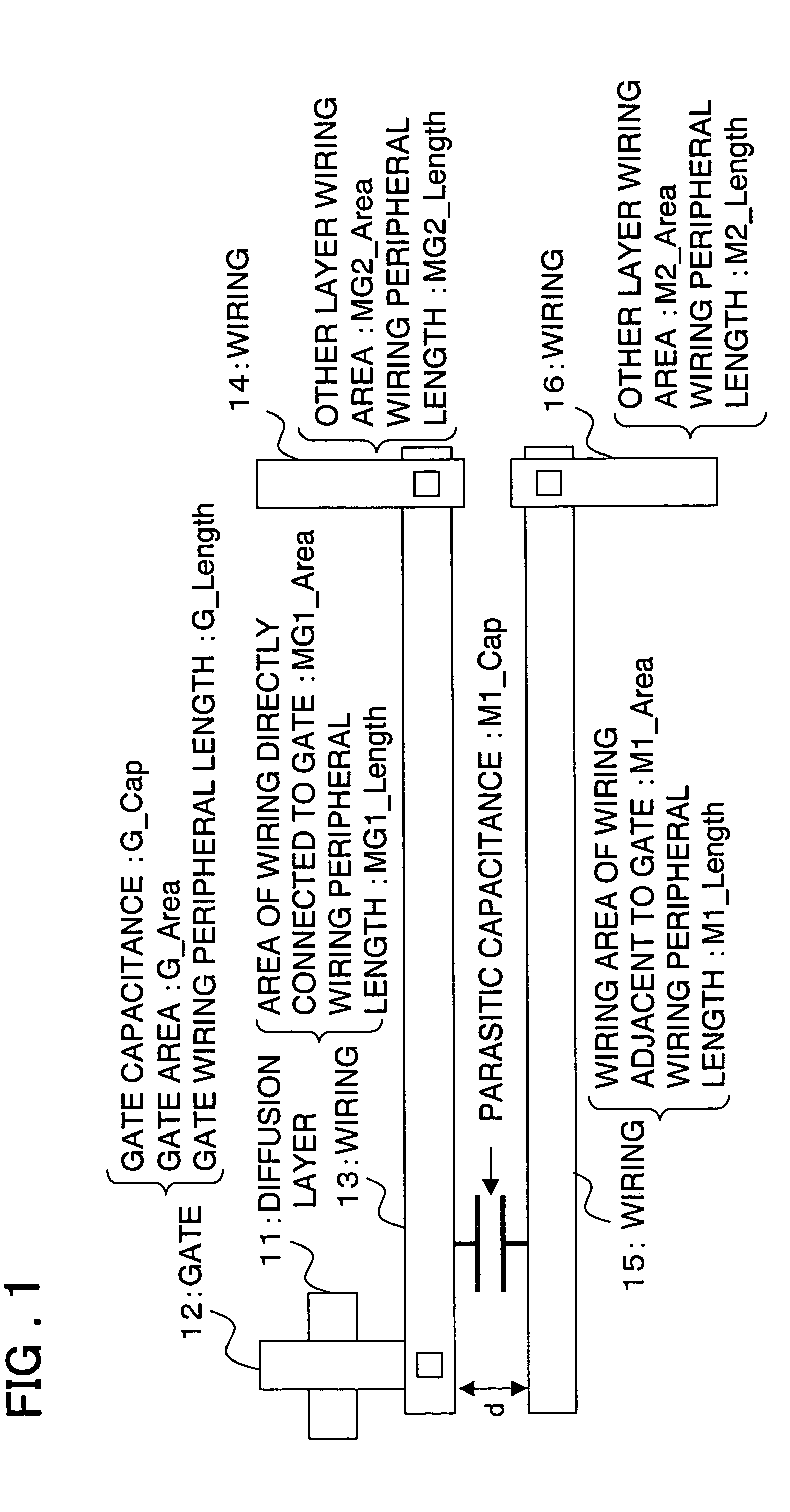
[0055]FIG. 2 is a diagram showing a layout of a semiconductor integrated circuit according to a second embodiment of the present invention. Referring to FIG. 2, the same reference numerals as those in FIG. 1 indicate components identical to or corresponding to those in FIG. 1. The layout shown in FIG. 2 is different from the layout in FIG. 1 in that a wiring 17 is added. The wiring 17 is arranged in parallel with the wiring 16 in other layer, and the area of the wiring 17 is indicated by M22_Area. Further, a parasitic capacitance between the wiring 16 and the wiring 17 is indicated by M22_Cap.

[0056]An antenna ratio R3 calculated from the areas and the capacitances in a configuration as described above is given by R3=All_Metal_Area / G_Area, in which All_Metal_Area=(MG1_Area+MG2_Area)+α (M1_Area+M2_Area)+β (M22_Area), and α is the parameter α=f1(G_Cap, M1_Cap) determined by a function f1 of the G_Cap and the M1_Cap. β is the parameter β=f2 (G_Cap, M1_Cap, M22_Cap) determined by a funct...

third embodiment

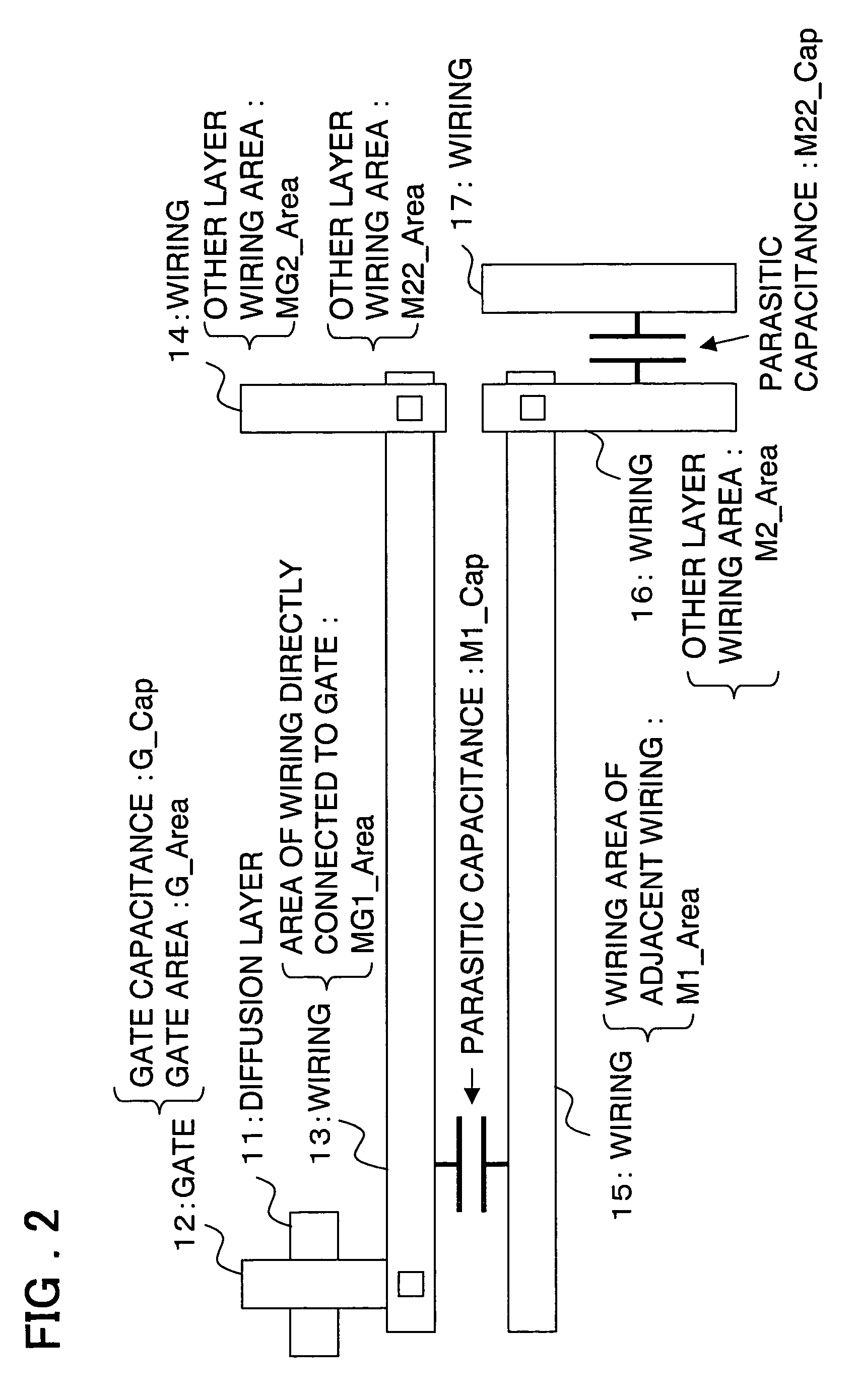
[0059]FIG. 3 is a diagram showing a layout of a semiconductor integrated circuit according to a third embodiment of the present invention. Referring to FIG. 3, the same reference numerals as those in FIG. 2 indicate components identical to or corresponding to those in FIG. 2. The layout shown in FIG. 3 is different from the layout in FIG. 2 in that a wiring 18, a wiring 19, a wiring 20, and a wiring 21 are added.

[0060]The wiring 18 is wired adjacent to and in parallel to the wiring 14 in other layer. The area of the wiring 18 is indicated by MG22_Area. A parasitic capacitance between the wiring 14 and the wiring 18 is indicated by MG22_Cap. The wiring 19 is wired adjacent to and in parallel with the wiring 15, and the area of the wiring 19 is indicated by M3_Area. A parasitic capacitance between the wiring 15 and the wiring 19 is indicated by M3_Cap. The wiring 20 is wired connected to the wiring 19 in other layer, and the area of the wiring 20 is indicated by M4_Area. The wiring 21...


PUM


Abstract

Semiconductor integrated circuit that prevents breakdown and degradation of a gate oxide film caused by charge-up in manufacturing steps thereof is provided. The circuit includes a gate 12 provided insulated from a transistor diffusion layer 11, wirings 13 and 14 connected to the gate 12, a wiring 15 parallel to and adjacent to the wiring 13, and a wiring 16 connected to the wiring 15. The gate area of the gate 12 is indicated by G_Area, and the gate capacitance of the gate 12 is indicated by G_Cap. The areas of the wirings 13, 14, 15, and 16 are indicated by MG1_Area, MG2_Area, M1_Area, and M2_Area, respectively, and a parasitic capacitance between the wirings 13 and 15 is indicated by M1_Cap. An antenna ratio R1 calculated from the areas is given by an equation R1={(MG1_Area+MG2_Area)+α(M1_Area+M2_Area)} / G_Area. α is a parameter determined by a function of the G_Cap and the M1_Cap. Layout of the wirings is performed so that a relation R1<L1 (which is a specified value that causes damage to a gate oxide film).

Description

FIELD OF THE INVENTION[0001]The present invention relates to a semiconductor integrated device, a design method thereof, a designing apparatus thereof, a program thereof, a manufacturing method thereof, and a manufacturing apparatus thereof. More specifically, the invention relates to the semiconductor integrated device for preventing breakdown and degradation of a gate oxide film caused by charge-up in manufacturing steps thereof, design method thereof, designing apparatus thereof, program thereof, manufacturing method thereof, and manufacturing apparatus thereof.BACKGROUND OF THE INVENTION[0002]In manufacturing steps of semiconductor integrated circuits, a technology employing plasma or an ion beam is used. In such steps, when a wiring of the semiconductor integrated circuit is the one that is not connected to a diffusion layer connected to a gate electrode, charges are accumulated on the wiring. Then, the amount of the charges exceeds a certain amount, the breakdown or degradatio...

Claims


Application Information

Patent Timeline
Patent Type & Authority Patents(United States)
IPC IPC(8): G06F17/50
CPCG06F17/5077H01L23/5222H01L27/0203H01L2924/0002H01L2924/00G06F30/394H01L21/18H01L27/02
Inventor FURUKI, TSUTOMU
Owner RENESAS ELECTRONICS CORP
Why Eureka
Try Eureka