Image sensor with a waveguide tube and a related fabrication method

a waveguide tube and image sensor technology, applied in the direction of diodes, semiconductor devices, electrical apparatus, etc., can solve the problems of crosstalk effect reducing cis imaging sensitivity, surface defects, increasing leakage current, etc., to prevent surface defects, increase image sensing efficiency and sensitivity, and different refractive indices

Active Publication Date: 2009-04-28
UNITED MICROELECTRONICS CORP
View PDF11 Cites 26 Cited by
  • Summary
  • Abstract
  • Description
  • Claims
  • Application Information

AI Technical Summary

Benefits of technology

[0010]It is therefore a primary objective of the present invention to provide an image sensor having at least a wave-guide tube for preventing a crosstalk effect and to increase sensitivity, and also to provide a method for fabricating the image sensor.
[0013]The image sensor of the present invention comprises at least a wave-guide tube having a concave bottom, which is positioned relative to the optical device at a predetermined distance. This prevents surface defects in the optical device and leakage current. The wave-guide tube further comprises an optical barrier to prevent the crosstalk effect between different optical paths. The optical barrier and the filler have different refractive indices, such that incident light striking at a non-perpendicular angle undergoes total internal reflection in the wave-guide tube. This results in a wave-guide effect. Therefore, the optical device collects more valid light beams to increase image sensing efficiency and sensitivity. The filler may be formed of dichroic film or a color filter to shorten a light path and to enhance a resolution of the image sensor.

Problems solved by technology

And, obviously, the crosstalk effect reduces CIS imaging sensitivity.
This results in surface defects and increases leakage current.

Method used


Image

  • Image sensor with a waveguide tube and a related fabrication method
  • Image sensor with a waveguide tube and a related fabrication method
  • Image sensor with a waveguide tube and a related fabrication method

Examples


Embodiment Construction

[0020]In the following detailed description, reference is made to the accompanying drawings, which form a part of this application. The drawings show, by way of illustration, specific embodiments in which the invention may be practiced. It is to be understood that other embodiments may be utilized and structural changes may be made without departing from the scope of the present invention.

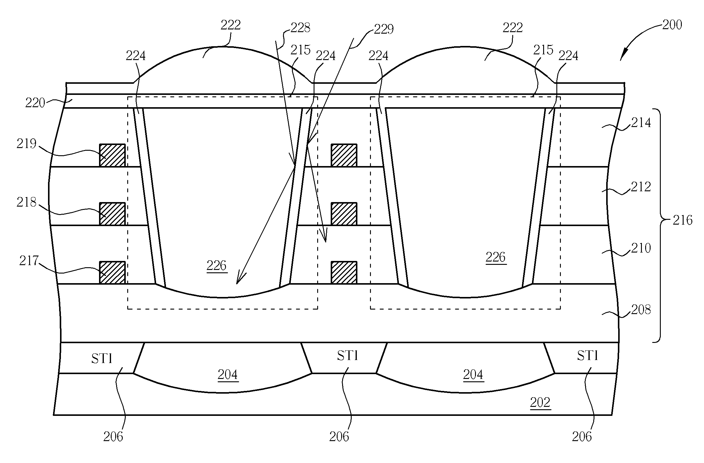
[0021]FIGS. 4 to 10 are schematic diagrams illustrating a method of fabricating an image sensor according to a preferred embodiment of the present invention. A substrate 100 is provided wherein at least an optical device 106 is formed, and at least an insulator 105 separates the optical device 106. At least an interlevel dielectric (ILD) layer 112 and a plurality of intermetal dielectric (IMD) layers 114, 116 and 118 are formed on the substrate 100, and a plurality of metal lines 107, 108 and 109 are formed in the IMD layers 114,116 and 118. In the preferred embodiment, the substrate 100 is a semic...


PUM


Abstract

An image sensor includes a substrate, at least an optical device, at least a dielectric layer, and at least a wave-guide tube disposed upon the optical device. The wave-guide tube has an optical barrier disposed on a sidewall thereof and a filter layer filled in the wave-guide tube. The structure of the wave-guide tube has the advantages of shortening light path, focusing, and preventing undesirable crosstalk effect between different optical devices.

Description

BACKGROUND OF THE INVENTION[0001]1. Field of the Invention[0002]The present invention is related to integrated image sensors, and more particularly, the present invention teaches an image sensor that uses a wave-guide tube.[0003]2. Description of the Prior Art[0004]CMOS image sensors (CIS) are popular image sensors at present. CIS fabrication can be integrated into conventional semiconductor processes, and therefore CIS has advantages of low cost, tiny size, and high integration. CIS also has advantages of low operating voltage, less power consumption, high quantum efficiency, low read-out noise, and random access. Therefore, CIS is adopted broadly in electronic products, such as PC cameras and digital cameras.[0005]A conventional CIS structure may be divided by function into a light sensing area and a peripheral electronic circuit area. The light sensing area has a plurality of photodiodes arranged in an array, and MOS transistors to sense light intensity, i.e. a reset transistor, ...

Claims


Application Information

Patent Timeline
Patent Type & Authority Patents(United States)
IPC IPC(8): H01L21/00H01L31/0232
CPCH01L27/14621H01L27/14625H01L27/14627H01L27/14685H01L27/14689H01L27/14643
Inventor KO, TENG-YUANPENG, NIEN-TSUCHEN, KUEN-CHU
Owner UNITED MICROELECTRONICS CORP
Why Eureka
Try Eureka