Reduced inductance interconnect for enhanced microwave and millimeter-wave systems

a technology of inductance interconnect and microwave and millimeter wave, which is applied in the direction of semiconductor devices, semiconductor/solid-state device details, nano-scale devices, etc., can solve the problems of limiting factor, flip chips, and the length of the interconnect coupling each radiator fin to an integrated circuit, and achieve the effect of reducing the inductance of an interconnect, eliminating or greatly reducing the disadvantages and problems associated

Active Publication Date: 2009-05-05
RAYTHEON CO
View PDF9 Cites 2 Cited by
  • Summary
  • Abstract
  • Description
  • Claims
  • Application Information

AI Technical Summary

Benefits of technology

[0004]In accordance with the present invention, a system and method for reducing the inductance of an interconnect is provided that substantially eliminates or greatly reduces disadvantages and problems associated with conventional microwave modules.
[0005]According to one embodiment of the present invention, a microwave or millimeter wave module includes a dielectric layer having a pocket formed substantially through the dielectric layer. The dielectric is attached to a metal substrate. The pocket has substantially vertical sidewalls. An integrated circuit is disposed in the pocket. Opposing sides of the integrated circuit are substantially parallel to the sidewalls of the pocket. An interconnect electrically couples the integrated circuit to a bond pad disposed on the outer surface of the dielectric layer. The interconnect has a length that is minimized to result in reduced inductance of the semiconductor device.
[0006]Certain examples of the invention may provide one or more technical advantages. A technical advantage of one exemplary embodiment of the present invention is that an integrated circuit may be disposed in a pocket. As a result, the top surface of the integrated circuit may be substantially coplanar with the top surface of the dielectric material in which the integrated circuit is embedded. Another technical advantage may be that, the length of the interconnect coupling the integrated circuit to the dielectric substrate may be decreased. As a result, the inductance of the integrated system may be decreased and performance of the circuit may be improved. Another technical advantage may be that the integrated circuit is supported directly on a metal layer such that heat generated by the integrated circuit may be removed from the semiconductor system through the metal layer.
[0007]Still another technical advantage may be that the channel separation distance between channels in a radar system may be decreased to permit high frequency operation and meet design requirements. As a result, a higher density of channels may be accomplished and the number of radiator fins present in the radar system per square inch may be increased. Accordingly, the operating frequency of the radar system may be increased. For example, in particular embodiments, a radar system may be operated at a W-band frequency exceeding 95 gigahertz and may be formed to include 32 channels or more in a single monolithic package.

Problems solved by technology

The length of the interconnect coupling each radiator fin to an integrated circuit, however, is a limiting factor in the development of high frequency radar systems as very low inductive interconnections between devices important for high-frequency applications.
Flip chips, however have their disadvantages.
This results in complex fabrication process and / or compromise in performance.
Further, the bumps formed on the surface of the integrated circuit to bond the flipped integrated circuit to the substrate are expensive to form and require complex assembly techniques.
Additionally, because coolant flow used to dissipate heat from an integrated circuit is removed from the semiconductor surface in a flip chip design, radar systems incorporating flip chips have thermal failure problems resulting from the inefficiency and inability of the active device to dissipate heat.
High operating temperatures result in reduced performance of the flip chip and the substrate supporting the flip chip.

Method used


Image

  • Reduced inductance interconnect for enhanced microwave and millimeter-wave systems
  • Reduced inductance interconnect for enhanced microwave and millimeter-wave systems
  • Reduced inductance interconnect for enhanced microwave and millimeter-wave systems

Examples


Embodiment Construction

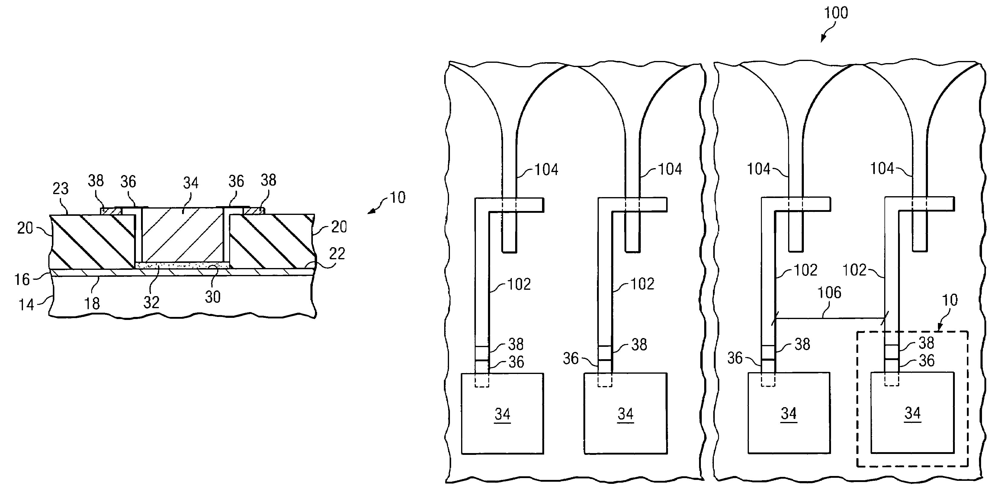
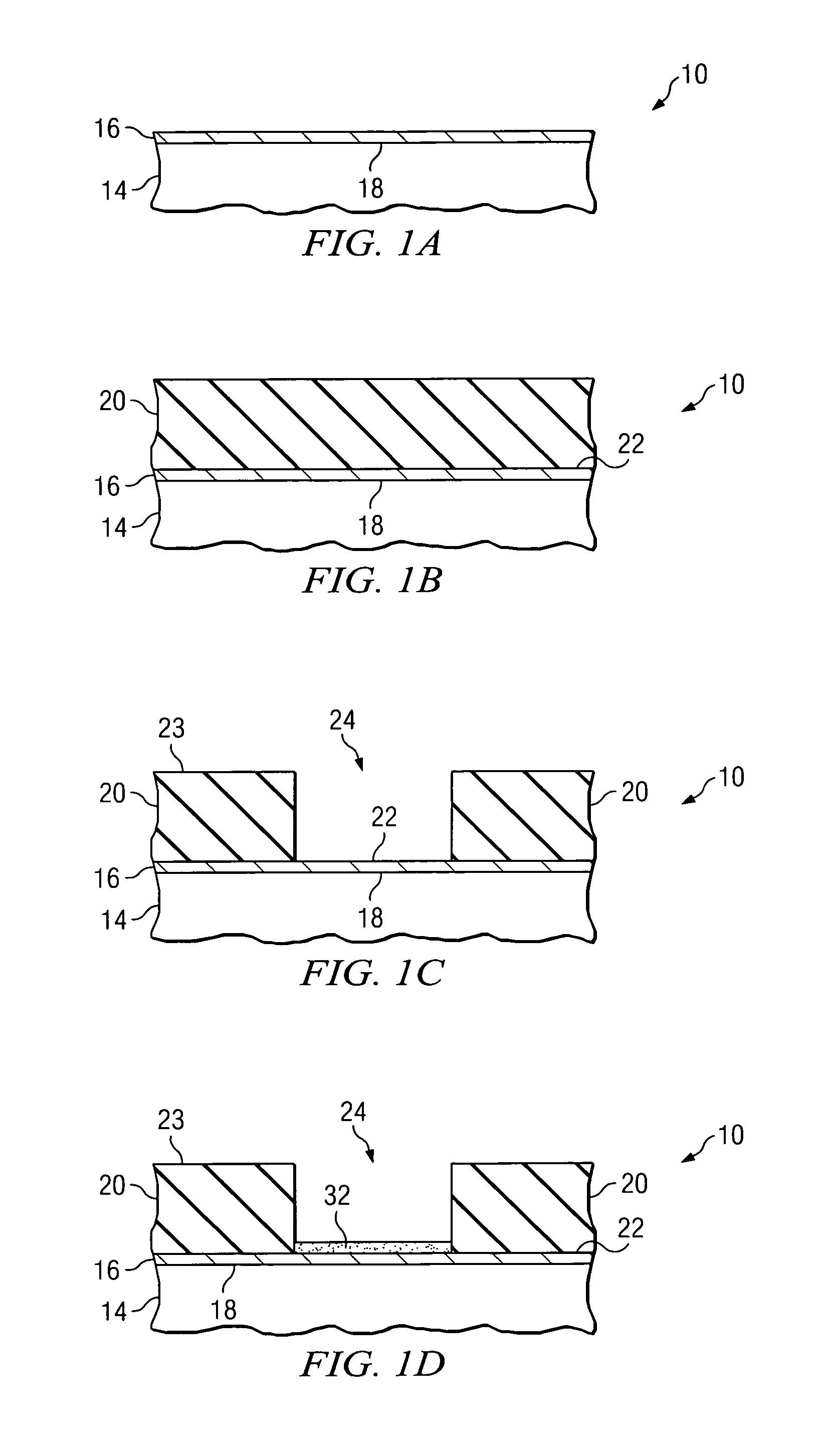
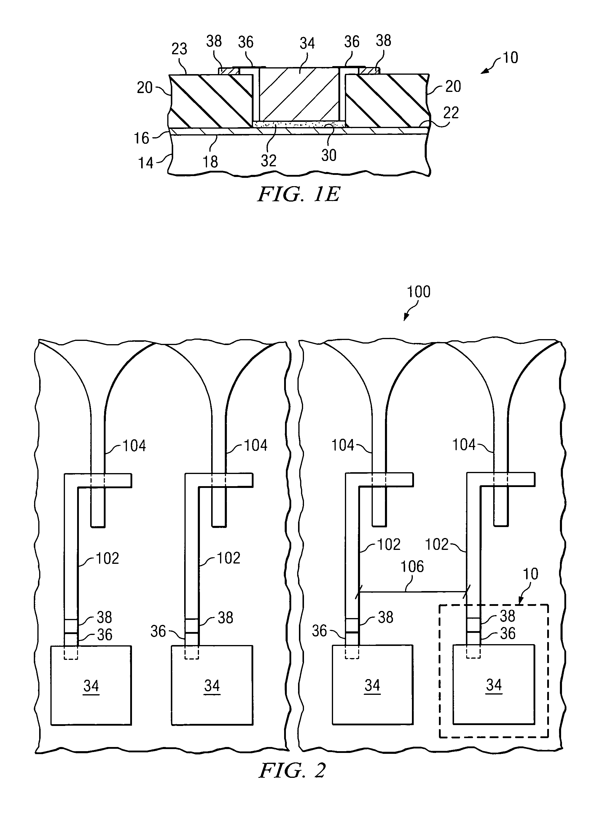
[0012]In order to form a radar system or other microwave or millimeter wave system, various conductive and nonconductive layers are typically formed on a suitable thermal substrate or other non-thermal substrate. FIGS. 1A-1E are cross-sectional views of an example microwave and / or millimeter wave structure (“microwave / millimeter wave structure”) 10 during the formation of multiple layers on an outer surface of a metal layer 14. Semiconductor microwave / millimeter wave structure 10 may be used as a basis for forming any of a variety of microwave / millimeter wave devices, such as a radar system incorporated into a missile or other aerospace platform or other high frequency communication system. Particular examples and dimensions specified throughout this document are intended for exemplary purposes only, and are not intended to limit the scope of the present disclosure. Moreover, the illustrations in FIGS. 1A-1E are not intended to be to scale. As will be discussed in more detail below,...


PUM


Abstract

According to one embodiment of the present invention, a microwave or millimeter wave module includes a dielectric layer having a pocket formed substantially through the dielectric layer. The dielectric is attached to a metal substrate. The pocket has substantially vertical sidewalls. An integrated circuit is disposed in the pocket. Opposing sides of the integrated circuit are substantially parallel to the sidewalls of the pocket. An interconnect electrically couples the integrated circuit to a bond pad disposed on the outer surface of the dielectric layer. The interconnect has a length that is minimized to result in reduced inductance of the semiconductor device.

Description

FIELD OF INVENTION[0001]The present invention relates generally to packaging microwave and millimeter wave devices and more particularly to a reduced inductance interconnect for enhancing microwave and millimeter-wave system performance.BACKGROUND OF THE INVENTION[0002]A radar system typically includes an array of transmit and receive modules / elements, which may be referred to as radiator fins, electrically coupled to an array of associated integrated microwave circuits. Typically, each radiator fin is coupled to an associated integrated circuit by a combination of an electrical channel through an interconnect. Although radar systems typically operate in the X to K band at a frequency on the order of 10 to 35 gigahertz, in some applications it may be desirable to operate a radar system at higher operating frequencies. To operate a radar at high frequencies, however, the radar must include a greater number of radiator fins per square inch. Accordingly, the size of components within t...

Claims


Application Information

Patent Timeline
Patent Type & Authority Patents(United States)
IPC IPC(8): H01Q21/00H01P1/00
CPCH01L23/66H01L24/83H01L2223/6611H01L2224/45014H01L2224/83851H01L2924/01004H01L2924/01014H01L2924/01078H01L2924/01079H01L2924/14H01L2924/1616H01L2924/19051H01L2924/30107H01L2924/3011H01L2224/2919H01L2924/01013H01L2924/01019H01L2924/01028H01L2924/0665H01L2924/00014H01L2224/48101H01L2224/73265H01L2224/85207H01L2924/206
Inventor MASON, JAMES S.BEDINGER, JOHN MICHAELRAJENDRAN, RAJ
Owner RAYTHEON CO
Why Eureka
Try Eureka