Vacuum conveying apparatus and charged particle beam equipment with the same

a technology of vacuum conveying apparatus and chargeable particle beam, which is applied in the direction of particle separator tubes, beam/ray deflecting arrangements, chemical vapor deposition coatings, etc., can solve the problems of prolonging waiting time, and achieve the effects of simplifying the structure, shortening the transfer time, and enhancing throughpu

Active Publication Date: 2009-05-12
HITACHI HIGH-TECH CORP
View PDF7 Cites 3 Cited by
  • Summary
  • Abstract
  • Description
  • Claims
  • Application Information

AI Technical Summary

Benefits of technology

[0022]Thus, the larger the internal space volume of the load lock chambers 82a, 82b is, the longer the waiting time by which the pressure therein is returned to a predetermined vacuum condition from a atmospherically opened condition is.
[0044]Further, in an embodiment form of the present invention, the auxiliary exhaust chamber has a volume which can be restrained to such a size that a sample such as a semiconductor wafer or the like can be accommodated therein and which can transfer the sample, thereby it is possible to allow the auxiliary exhaust chamber to have a volume which is necessary but minimum. Thus, the footprint saving can be made while the time of exhaustion from the auxiliary exhaust chamber can be greatly shortened. Further, since no elevation drive portion is present in the auxiliary exhaust chamber, it is possible to restrain occurrence of foreign matter such as dust and dirt which cause contamination.

Problems solved by technology

Thus, there would have been possibly caused a problem of prolonging the waiting time.

Method used


Image

  • Vacuum conveying apparatus and charged particle beam equipment with the same
  • Vacuum conveying apparatus and charged particle beam equipment with the same
  • Vacuum conveying apparatus and charged particle beam equipment with the same

Examples


embodiment 1

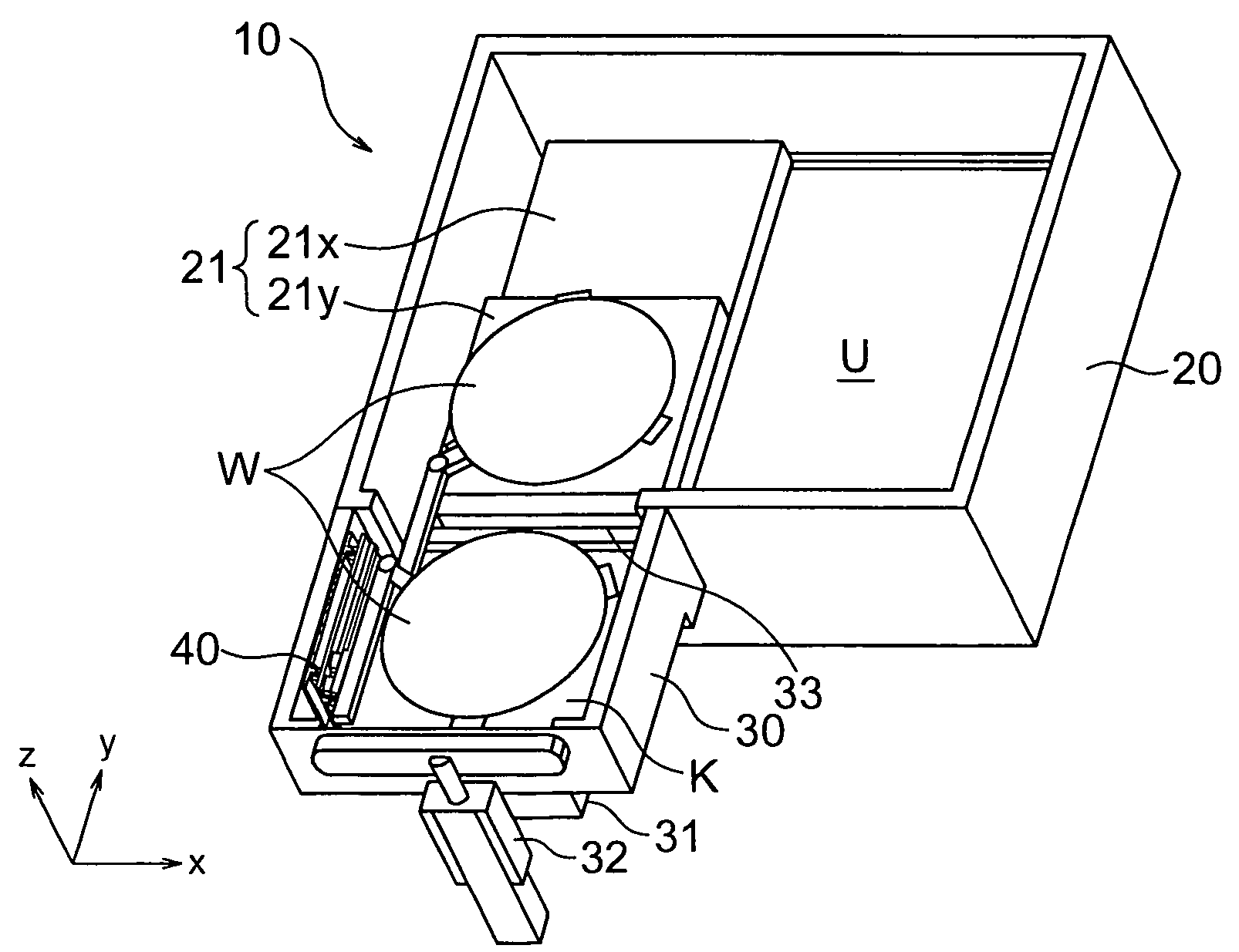
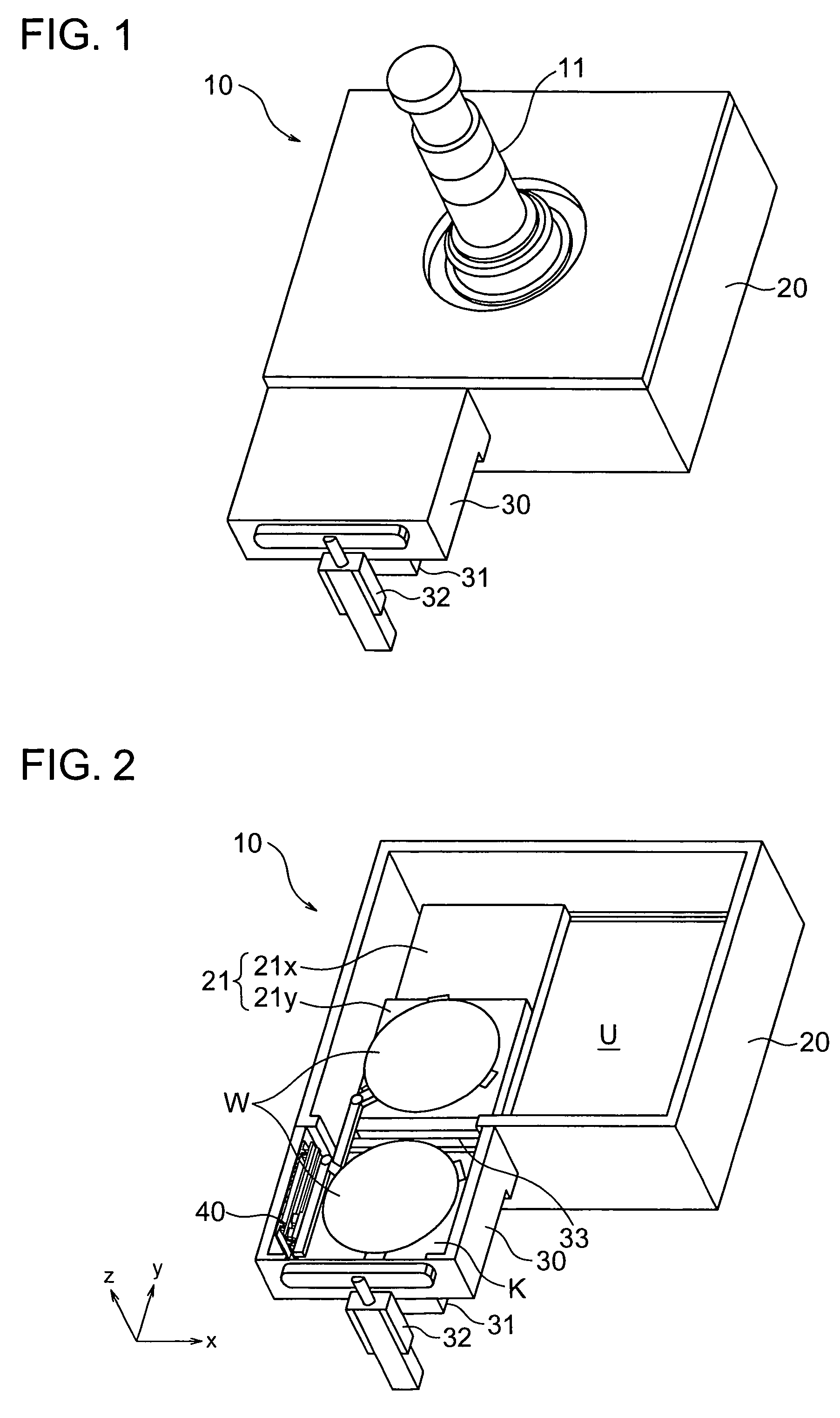
[0064]Explanation will be hereinbelow made of embodiments of the present invention with reference to the accompanying drawings. Referring to FIG. 1, an electron microscope 10 comprises an electron optical system column 11, a sample chamber 20 and a load lock chamber 30. It is noted that explanation will be made of the electron microscope as an example of the charged particle beam equipment in this embodiment. However, the present invention should not be limited to this embodiment, that is, the present invention may also be applied to a focused ion beam apparatus (FIB) in which an ion beam is irradiated onto a sample so as to carry out processing, observing, examining, measuring or the like of the sample.

[0065]The electron optical system column 11 is provided in a substantially center part of the upper surface of the sample chamber 20, for irradiating a focused beam toward a wafer set in the internal space of the sample chamber 20 as shown in FIG. 1.

[0066]The electron optical system ...

embodiment 2

[0112]FIG. 10 is a perspective view illustrating an embodiment of a vacuum transfer apparatus according to the present invention, FIG. 11 is a schematic sectional view illustrating the vacuum transfer apparatus shown in FIG. 10, and FIG. 12 is a schematic perspective view illustrating a power transmission mechanism in the above vacuum transfer apparatus in an example form.

[0113]As shown in FIG. 10, the vacuum transfer apparatus 126 is provided with on the vacuum N side (Refer to FIG. 11) an arm 101 which is supported so that it can be rotated and vertically moved by two drive sources 102, 110 arranged on the atmospheric M side (Refer to FIG. 11) for rotation and vertical motions. A first hand 122 and a second hand 123 are rotatably supported respectively to opposite ends of the arm 101, and accordingly, they are rotated in association with the rotation of the arm 101 in order to carry a sample such as a semiconductor wafer 121. The rotation of the arm 101 is transmitted to each of t...


PUM

PropertyMeasurementUnit
sizeaaaaaaaaaa
angleaaaaaaaaaa
rotating angleaaaaaaaaaa

Abstract

A charged particle beam examination equipment for examining and measuring a semiconductor wafer, comprising a wafer exchange portion for exchanging an unexamined wafer and an examiner wafer with each other, which has a first arm longitudinally sliding for reciprocation, a first wafer gripping part provided to the distal end of the first arm, for gripping / releasing the wafer, a second arm longitudinally sliding for reciprocation, and a second wafer gripping part provided to the distal end of the second arm, for gripping / releasing the wafer. The apparatus may shorten the time required for exchange of the wafers so as to enhance the throughput during examination and measurement of the wafers.

Description

BACKGROUND OF THE INVENTION[0001]The present invention relates to a charged particle beam equipment for examining and measuring semiconductor wafers, and in particular, to a waver exchange mechanism.[0002]In an electron microscope for observing and examining an outer surface of a semiconductor wafer, it is required to rapidly exchange wafers to be examined having a size of up to 300 mm. Accordingly, it is required to shorten the waiting time until a next wafer to be examined is set in a sample chamber where a wafer is irradiated with a focused beam, after a preceding wafer is examined.[0003]Referring to FIG. 9, explanation will be made of the background technology.[0004]A wafer exchange-mechanism for wafers W (WA, WB) in a conventional electron microscope 80 comprises a sample chamber 81 in which a focused beam emitted from an electron optical system column 83 is irradiated to a wafer WA, and a plurality of load lock chambers 82a, 82b (two chambers in the case shown in the figure) w...

Claims


Application Information

Patent Timeline
Patent Type & Authority Patents(United States)
IPC IPC(8): G01F23/00G01K5/08G01K5/10
CPCH01J37/18H01L21/67201H01L21/67742H01L21/67748H01J2237/204Y10S277/913Y10S414/139
Inventor SAITO, HIROYUKITOMIDA, SHOUJI
Owner HITACHI HIGH-TECH CORP
Why Eureka
Try Eureka