Uniform etching system and process for large rectangular substrates

a rectangular substrate, uniform technology, applied in the direction of coatings, chemical vapor deposition coatings, electric discharge tubes, etc., can solve the problems of large electrical potential variations across the surface of the larger substrate, difficult to achieve the uniform rate needed for good device yield, and large potential differences, etc., to achieve the effect of improving the control of the uniformity of etching rate and/or substrate surface electrical potential

Inactive Publication Date: 2009-05-19
SAVAS STEPHEN E
View PDF5 Cites 5 Cited by
  • Summary
  • Abstract
  • Description
  • Claims
  • Application Information

AI Technical Summary

Benefits of technology

[0012]These and other objects are achieved in accordance with the invention by providing a showerhead that provides improved control of the uniformity of etching rate and / or substrate surface electrical potential in an etching or substrate cleaning reactor utilizing an rf discharge between substantially parallel plates for processing large rectangular substrates. The showerhead includes a reservoir connected by a plurality of small holes to the volume between the plates wherein the discharge is sustained, two or more gas injection manifolds connected through flow controlling means to supplies of different process gases or mixtures, with each of the two or more gas injection manifolds having a different spatial pattern of members, and different distribution of openings for releasing gas or mixture of gases that they carry into the volume of the reservoir with differing spatial and or temporal distributions.

Problems solved by technology

There are many significant technical problems with scaling well-known methods for dry etching and photoresist ashing to the very large substrates such as fifth generation TFT / LCD (thin film transistor liquid crystal display) flat panel substrates or large solar panels.
However, with increasing substrate size and a rectangular shape, it is increasingly difficult to achieve the uniformity of rate needed for good device yields.
In addition, RF plasma discharge processes are likely to cause substantial electrical potential variations across the surface of the larger substrates.
Such potential differences typically increase as the size of the substrate increases and also worsen as non-uniformities in the process increase.
Such potential variations can cause electrical stress damage to components being fabricated on the substrate.
Therefore, any variation in the spacing between the showerhead and pedestal is likely to cause non-uniformity in the etching rate, and can also cause substrate-charging problems as well.
With large showerheads or pedestals, maintaining a high degree of flatness after processing large numbers of substrates may be very challenging, and the problem is compounded because the relationship between electrode gap and etch rate is non-linear.
That, in turn, causes even further increase in RF current density in the areas.
However, good uniformity of etching rate has become increasingly difficult as the substrate or wafer size has increased.
Getting good uniformity of surface potential has been very difficult even for round wafers of limited size, and remains a significant challenge with this type of etching technology.
For the larger and larger rectangular substrates used for making TFT / LCD screens, it has not been possible to achieve satisfactory uniformity of etch rate by scaling up the traditional etching processes.
That approach is pretty much limited to round wafers, and it does not address the issue of uniform substrate surface potential which is very important for achieving good yields in devices having thin, sensitive dielectric layers.
Hence, concentric segmentation would not be very effective with a rectangular substrate.
That means that a very complex, iterative adjustment scheme would be needed to actually accomplish the adjustment of the rates desired.
Use of such a rate adjustment method and apparatus would increase cost and complexity of the device and still not be likely to be successful due to the variation of the rate across the area of each of the segments.
To be successful, such an approach would require a very large number of segments, possibly 25 or more, and would be prohibitively expensive.

Method used


Image

  • Uniform etching system and process for large rectangular substrates
  • Uniform etching system and process for large rectangular substrates
  • Uniform etching system and process for large rectangular substrates

Examples


Embodiment Construction

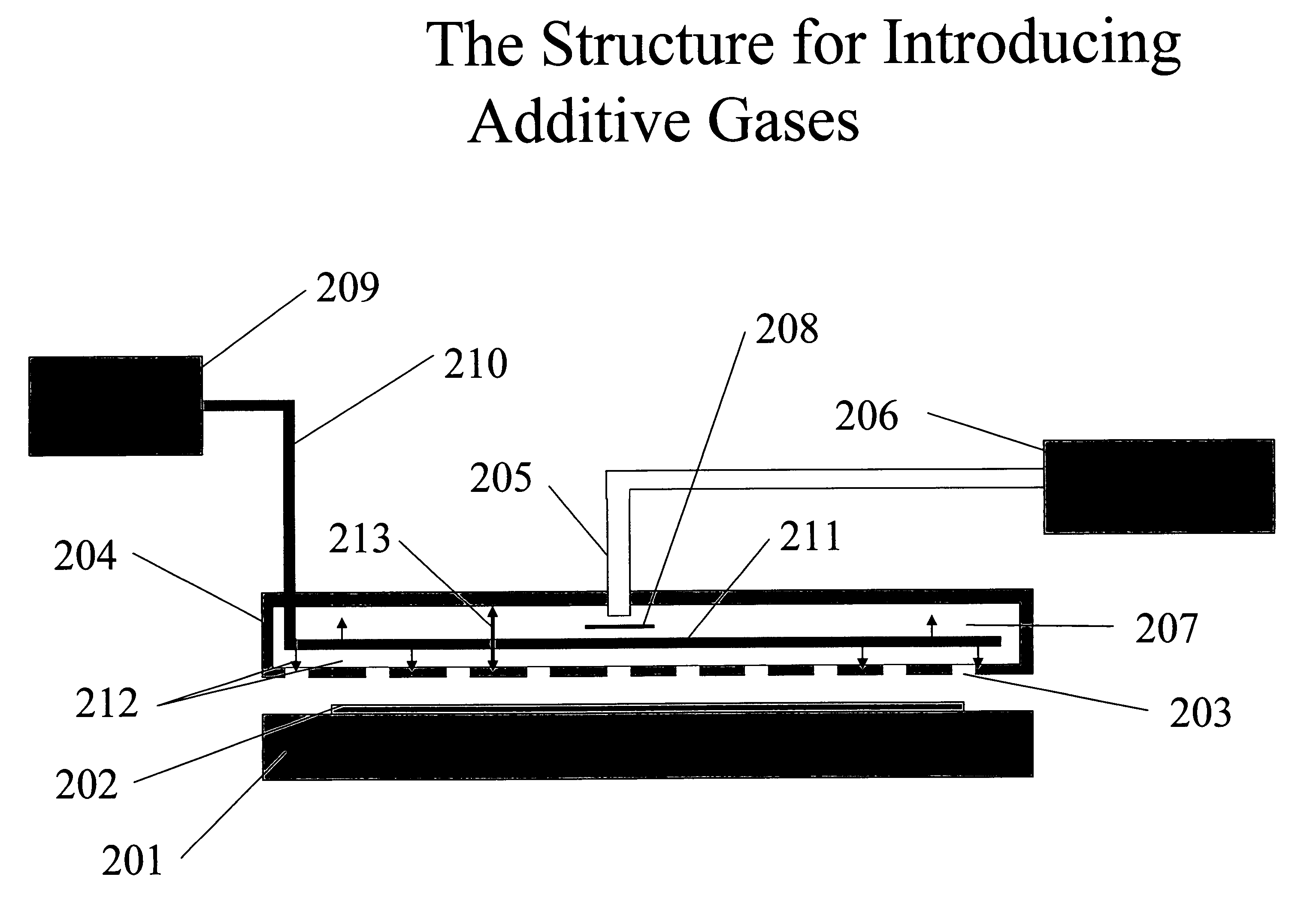
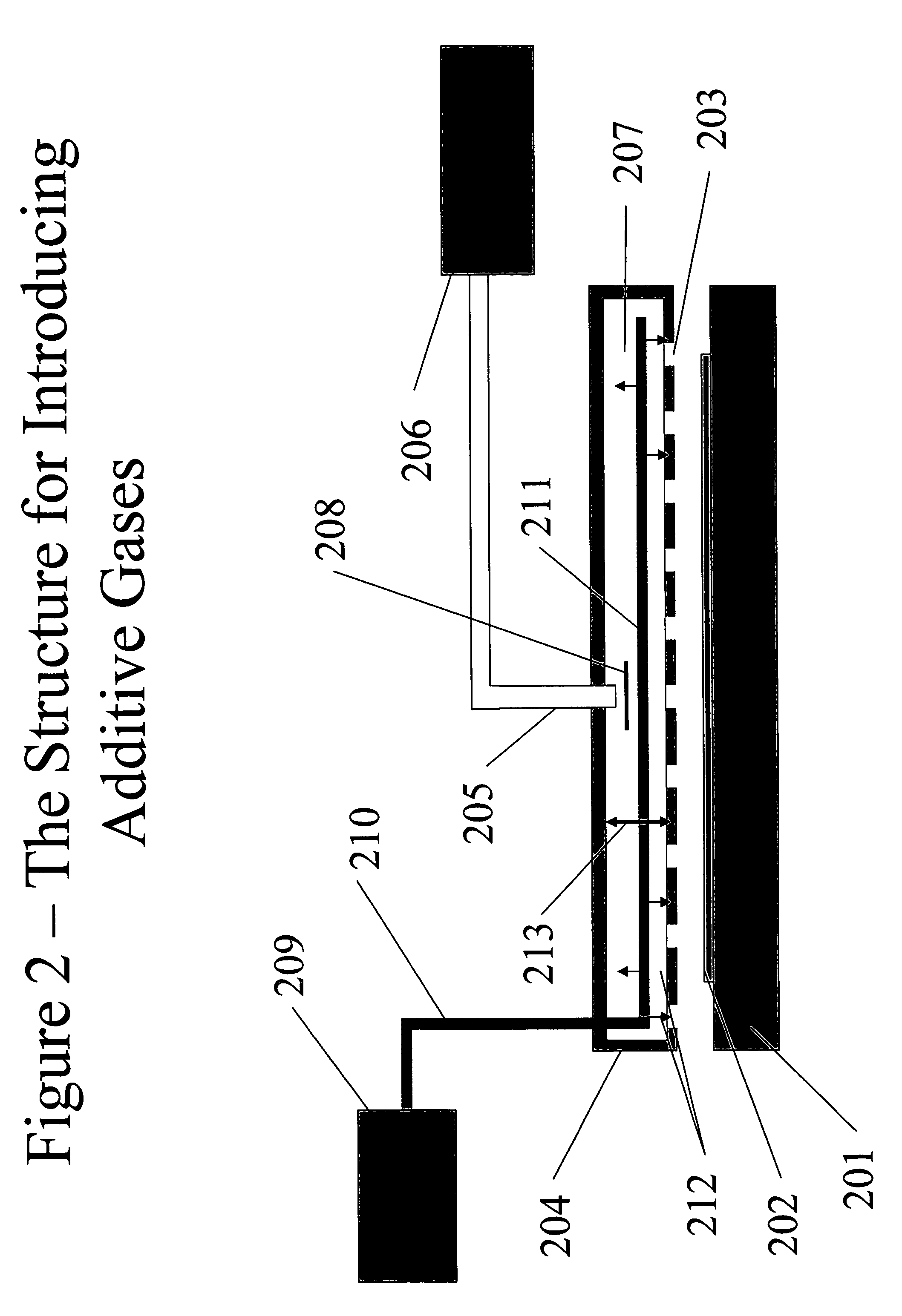
[0017]It has been observed that the etching rate across the large substrate varies in a reasonably well-behaved manner except at or near its corners. It has also been found that both the etching rate and the surface potential on the substrate must be adjusted to achieve good uniformity for many types of substrate manufacturing technologies, and that inert gases or other gases which do not greatly affect etching rate can affect the electrical potential on the panel surface. The invention provides a practical, relatively low cost apparatus and process for reducing the variation of both etching rate and surface potential across a large substrate.

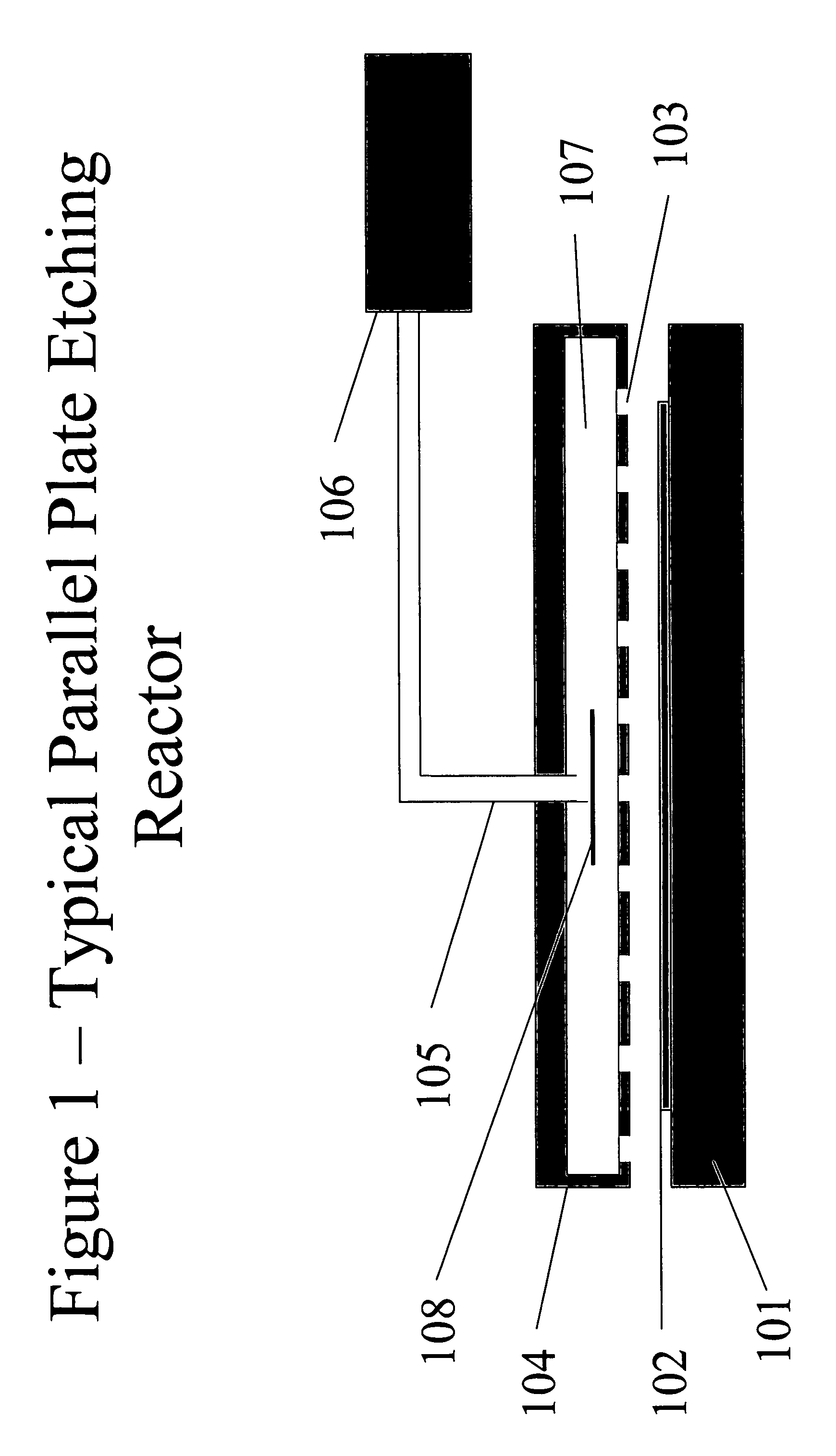
[0018]In parallel plate discharges for etching, where the showerhead for introducing gas(es) also serves as one of the electrodes, there has normally been a single primary reservoir feeding the gas mixture to the holes through which it flows into the discharge volume. This reservoir covers an area within the showerhead that extends on all sides...


PUM

PropertyMeasurementUnit
areaaaaaaaaaaa
concentrationaaaaaaaaaa
processing rateaaaaaaaaaa

Abstract

Apparatus and process for controlling etching of silicon-based or organic materials on large rectangular substrates for manufacture of flat panel displays or other devices. The disclosed etching process can remove silicon-based materials or organic polymers with a rate distribution such that all areas of the panel are finished at nearly the same time. It does so while minimizing electrical charging of the workpiece that could cause damage to the devices. The etching chamber employs a parallel plate RF discharge between two electrodes, one of which is the showerhead for gas introduction and the other supports the substrate to be processed. Reactant and other gases are provided to the discharge by a novel showerhead structure. The gases which provide reactants for etching silicon-based materials include halogenated compounds. Oxygen, water vapor or hydrogen with other gas additives may be used for etching organic polymers. The uniformity of etching across the substrate is controlled by adding other gas(es), including inert diluents, which can control the etching rate for either silicon-based materials or organic materials by accelerating and / or decreasing it. In addition, the distribution of the gases which are added can be varied to make the surface potential of the substrate more uniform. With a showerhead having a single reservoir that feeds all gases into the discharge, the gases may be added to the reservoir through multiple distribution structures within or adjacent to the reservoir. These structures are each supplied separately with the additive gases and, in turn, feed them to the different regions of the reservoir. The invention can thus provide different etching rates for different parts of the substrate, as may be required to finish film removal in all areas of the panel at nearly the same time. The invention also provides for chemical conversion of inorganic residues remaining after the oxidation of an organic polymer in the ashing process by addition of small amounts of halogenated gas(es) to the mixture flowing through the plasma sources. With the system and process of the invention, space efficiency, operating cost and capital cost for making large substrates can be reduced significantly.

Description

BACKGROUND OF THE INVENTION[0001]1. Field of Invention[0002]This invention pertains to a novel apparatus and process for controlling etching of silicon-based or organic materials on large rectangular substrates for manufacture of flat panel displays or other devices.[0003]2. Related Art[0004]There are many significant technical problems with scaling well-known methods for dry etching and photoresist ashing to the very large substrates such as fifth generation TFT / LCD (thin film transistor liquid crystal display) flat panel substrates or large solar panels. The best-known and least expensive approach for etching is with parallel plate, RF discharges such as have been used for decades in manufacturing integrated circuits. For ashing in IC manufacturing the proven parallel plate resist stripping method found in U.S. Pat. No. 5,189,634 was able to achieve good results and productivity for 200 mm wafers. However, with increasing substrate size and a rectangular shape, it is increasingly ...

Claims


Application Information

Patent Timeline
Patent Type & Authority Patents(United States)
IPC IPC(8): B44C1/22C03C15/00C03C25/68C23F1/00
CPCH01J37/32082H01J37/3244
Inventor SAVAS, STEPHEN E.
Owner SAVAS STEPHEN E
Why Eureka
Try Eureka