Monolithically integrated light emitting devices

a technology of light emitting devices and monoliths, applied in the direction of radiation control devices, layered products, basic electric elements, etc., can solve the problems of disrupting old markets, new markets as well, and affecting the development of new markets

Active Publication Date: 2009-05-19
MASSACHUSETTS INST OF TECH
View PDF46 Cites 225 Cited by
  • Summary
  • Abstract
  • Description
  • Claims
  • Application Information

AI Technical Summary

Problems solved by technology

The basic idea was that combining the ability to emit and detect light (III-V material) with digital logic (silicon digital circuits) would result in new markets as well as disrupt old markets.
However, actually accomplishing this goal in a practical way has proven more a challenge than was at first recognized.

Method used


Image

  • Monolithically integrated light emitting devices
  • Monolithically integrated light emitting devices
  • Monolithically integrated light emitting devices

Examples


Embodiment Construction

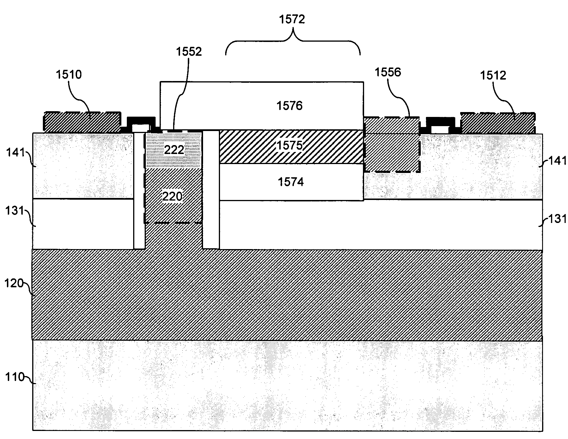
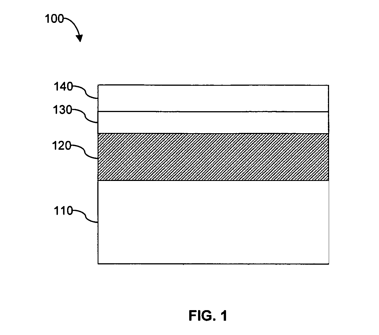
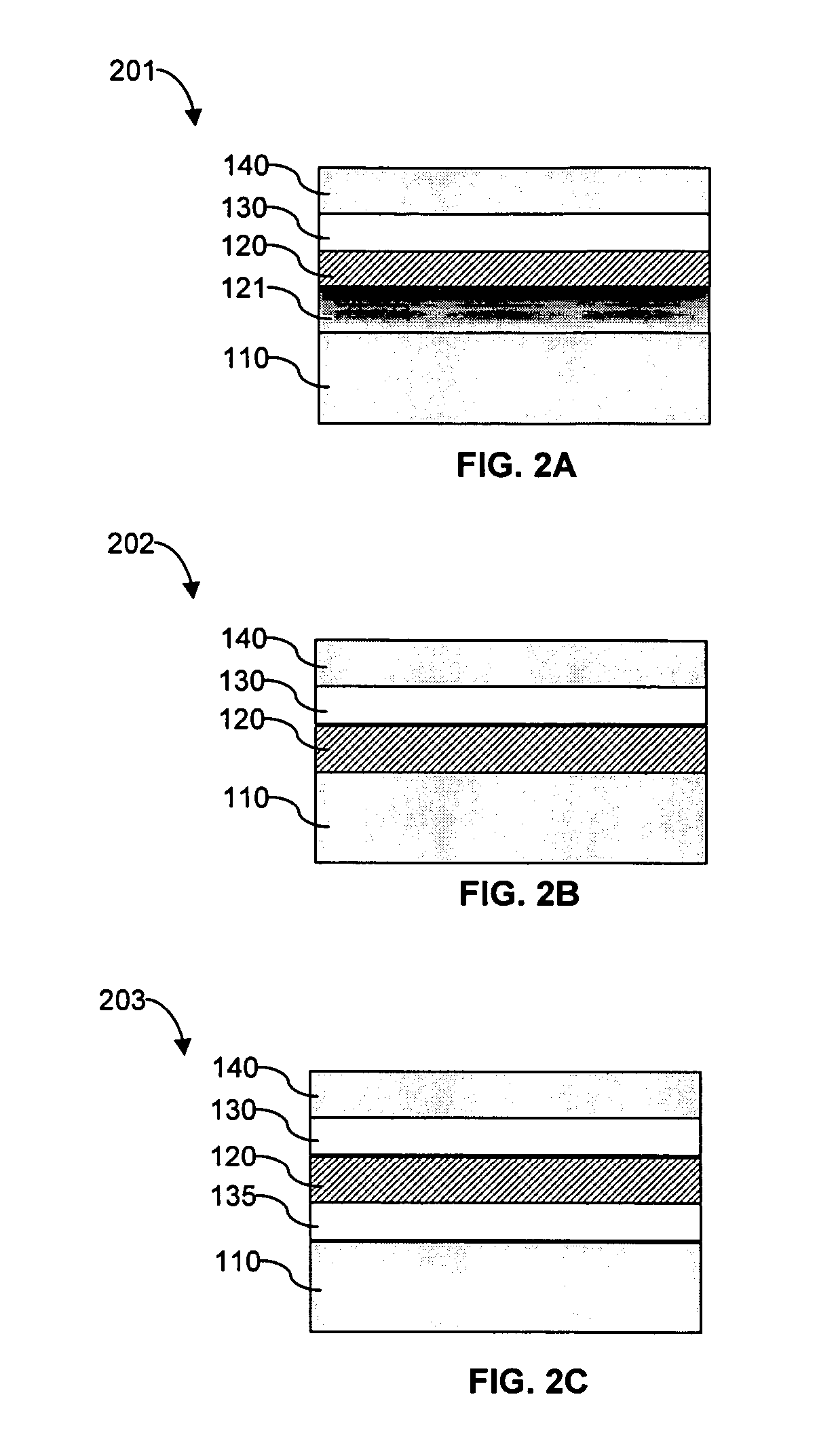
[0031]Embodiments presented herein provide examples of implementations of methods and structures to facilitate the monolithic integration of a silicon-based monocrystalline layer with one or more monocrystalline semiconductor layers having a lattice constant(s) other than that of relaxed silicon. In some embodiments, silicon-based devices are monolithically integrated with devices having active regions formed of one or more monocrystalline semiconductors having lattice constant(s) other than that of relaxed silicon. Silicon-based devices can include (but are not limited to) silicon-based electronics, such as n-type metal oxide semiconductor (NMOS) and p-type metal oxide semiconductor (PMOS) field effect transistors (FETs), complementary metal oxide semiconductor (CMOS) devices, and bipolar transistors. Silicon-based devices can also include optoelectronic devices, such as silicon-based photodetectors. Non-silicon semiconductor devices can include (but are not limited to) III-V light...


PUM


Abstract

Methods and structures for monolithically integrating monocrystalline silicon and monocrystalline non-silicon materials and devices are provided. In one structure, a monolithically integrated semiconductor device structure comprises a silicon substrate and a first monocrystalline semiconductor layer disposed over the silicon substrate, wherein the first monocrystalline semiconductor layer has a lattice constant different from a lattice constant of relaxed silicon. The structure further includes an insulating layer disposed over the first monocrystalline semiconductor layer in a first region and a monocrystalline silicon layer disposed over the insulating layer in the first region. The structure includes at least one silicon-based electronic device including an element including at least a portion of the monocrystalline silicon layer. The structure also includes a second monocrystalline semiconductor layer disposed over at least a portion of the first monocrystalline semiconductor layer in a second region and absent from the first region, wherein the second monocrystalline semiconductor layer has a lattice constant different from the lattice constant of relaxed silicon. The structure includes at least one III-V light-emitting device including an active region including at least a portion of the second monocrystalline semiconductor layer.

Description

RELATED APPLICATIONS[0001]This application claims priority under 35 U.S.C. § 119(e) to U.S. Provisional Application Ser. No. 60 / 732,442, entitled “INTEGRATED LIGHT ARRAYS,” filed on Nov. 1, 2005 and U.S. Application Ser. No. 60 / 790,204, entitled “INTEGRATED LIGHT ARRAYS,” filed on Apr. 7, 2006, which are herein incorporated by reference in their entirety.FIELD OF INVENTION[0002]This invention relates generally to the manufacture of semiconductor structures. More particularly the invention relates to the monolithic integration of silicon and other monocrystalline semiconductor materials and / or devices.BACKGROUND[0003]The concept of combining III-V materials with silicon was born in the 1980s. Although the degree of progress in silicon technology could not be anticipated at the time and therefore many potential applications could not be detailed, such technology was pursued on a fundamental basis. The basic idea was that combining the ability to emit and detect light (III-V material) ...

Claims


Application Information

Patent Timeline
Patent Type & Authority Patents(United States)
IPC IPC(8): H01L23/06H01L33/00H01L33/06H01L33/08H01L33/32
CPCH01L21/76254H01L21/8258H01L27/0605H01L27/144H01L27/1446H01L27/14601H01L27/14683H01L27/15H01L31/0328H01L31/143H01L31/162H01L21/0245H01L21/0251H01L27/156Y10S438/933H01L2924/0002H01L2924/00H01L21/20H01L31/113B32B9/04
Inventor FITZGERALD, EUGENE A.
Owner MASSACHUSETTS INST OF TECH
Why Eureka
Try Eureka