Embedded fiber acoustic sensor for CMP process endpoint

a technology of acoustic sensor and fiber acoustic sensor, which is applied in the direction of grinding machine components, manufacturing tools, lapping machines, etc., can solve the problems of reducing the processing throughput of cmp, affecting the accuracy of photolithographic processes used to form sub-micron features, and reducing the sensitivity of the sensor, so as to achieve high spatial mapping of the acoustic energy or vibration spectrum of the substrate, easy incorporation, and increased sensitivity

Active Publication Date: 2009-05-26
MICRON TECH INC
View PDF52 Cites 7 Cited by
  • Summary
  • Abstract
  • Description
  • Claims
  • Application Information

AI Technical Summary

Benefits of technology

[0013]The invention utilizes a fiber optic contact sensor for CMP process monitoring of mechanical energy (e.g., mechanical vibration) and acoustical energy (e.g., ultrasonic vibration) that allows an operator to determine status and / or an endpoint of a planarizing or polishing process.
[0023]Many CMP processes require a process endpoint based upon topography removal or degree of planarization, and transition from one film to the next, e.g., oxide to nitride. By incorporation of a fiber optic sensor into the CMP pad or CMP-subpad assembly or the CMP support table, increased sensitivity is gained to monitor acoustic energy or vibration signatures emanating from the wafer:pad interface during CMP processing. The present invention provides a non-obtrusive approach that can be readily incorporated into a CMP pad with sufficient density such that high spatial mapping of the substrate acoustic energy or vibration spectrum can be obtained with a high level of precision that is representative of the degree of planarization or process endpoint. The incorporation of an acoustic or vibrational sensor directly into a CMP pad or pad-subpad assembly provides improved spatial sensing to enable monitoring of wafer clearing as a function of discrete radii sections across the wafer. The invention advantageously reduces quality losses, and significantly increases productivity, throughput and yield.

Problems solved by technology

During fabrication, the substrate is typically planarized at various stages to make it level and uniform, and eliminate recesses, protrusions, scratches, and other undesirable topology, which can cause step coverage problems for the deposition of a subsequent material layer and depth of focus problems that impair photolithographic processes used to form sub-micron features.
This method may not produce accurate results due to differences in polishing rates and variations from one substrate to another.
However, interrupting a CMP process to remove the workpiece from the pad reduces CMP processing throughput and can cause damage to the workpiece.
However, incorporating sensors into the carrier poses problems with signal dampening.
Such a set-up is also not practical in manufacturing applications due to the need to isolate the carrier from the carrier using a urethane containing material, which leads to high signal attenuation.

Method used


Image

  • Embedded fiber acoustic sensor for CMP process endpoint
  • Embedded fiber acoustic sensor for CMP process endpoint
  • Embedded fiber acoustic sensor for CMP process endpoint

Examples


Embodiment Construction

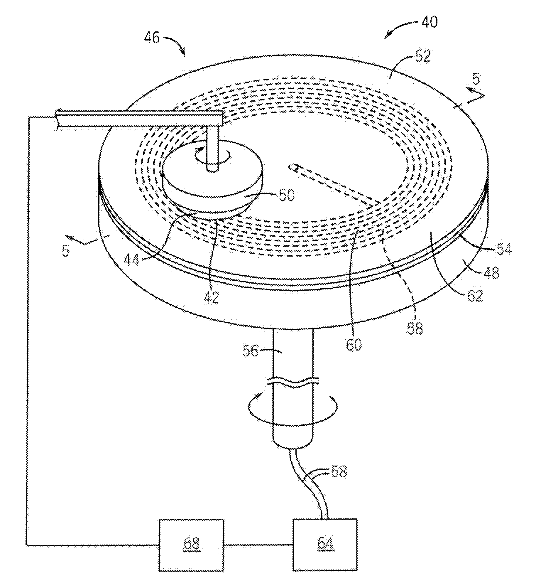
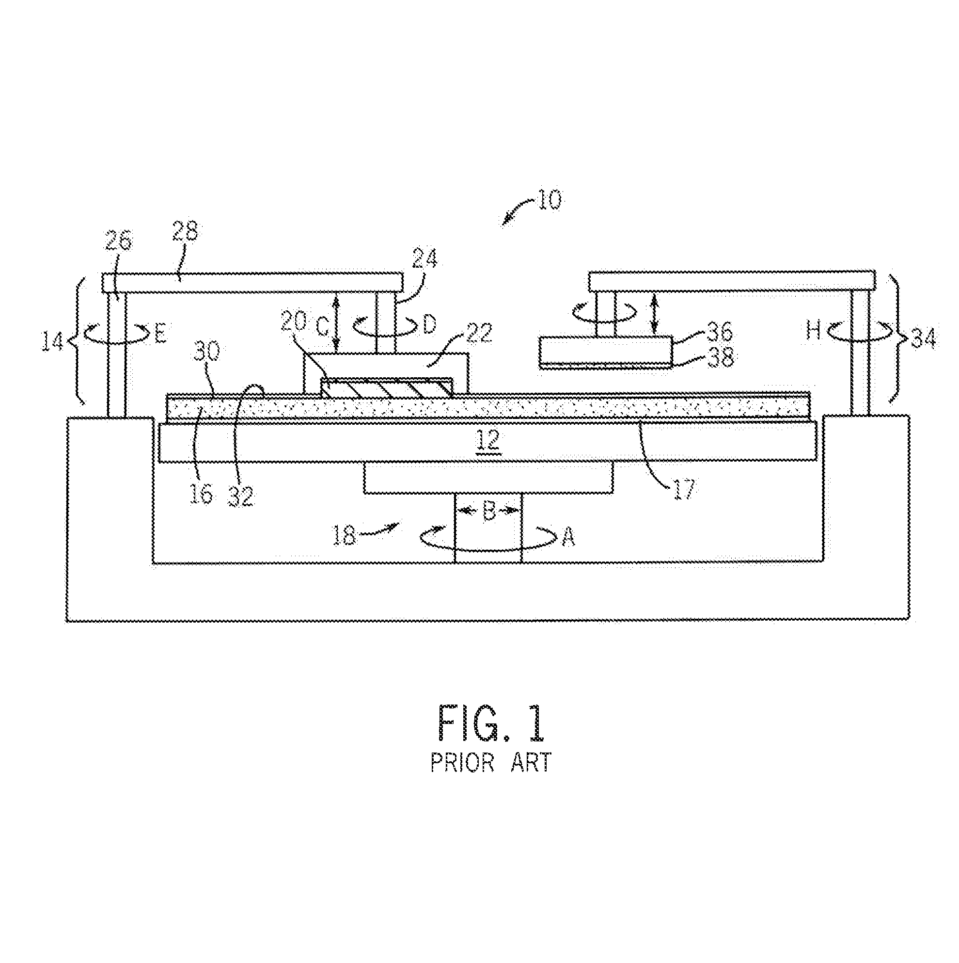
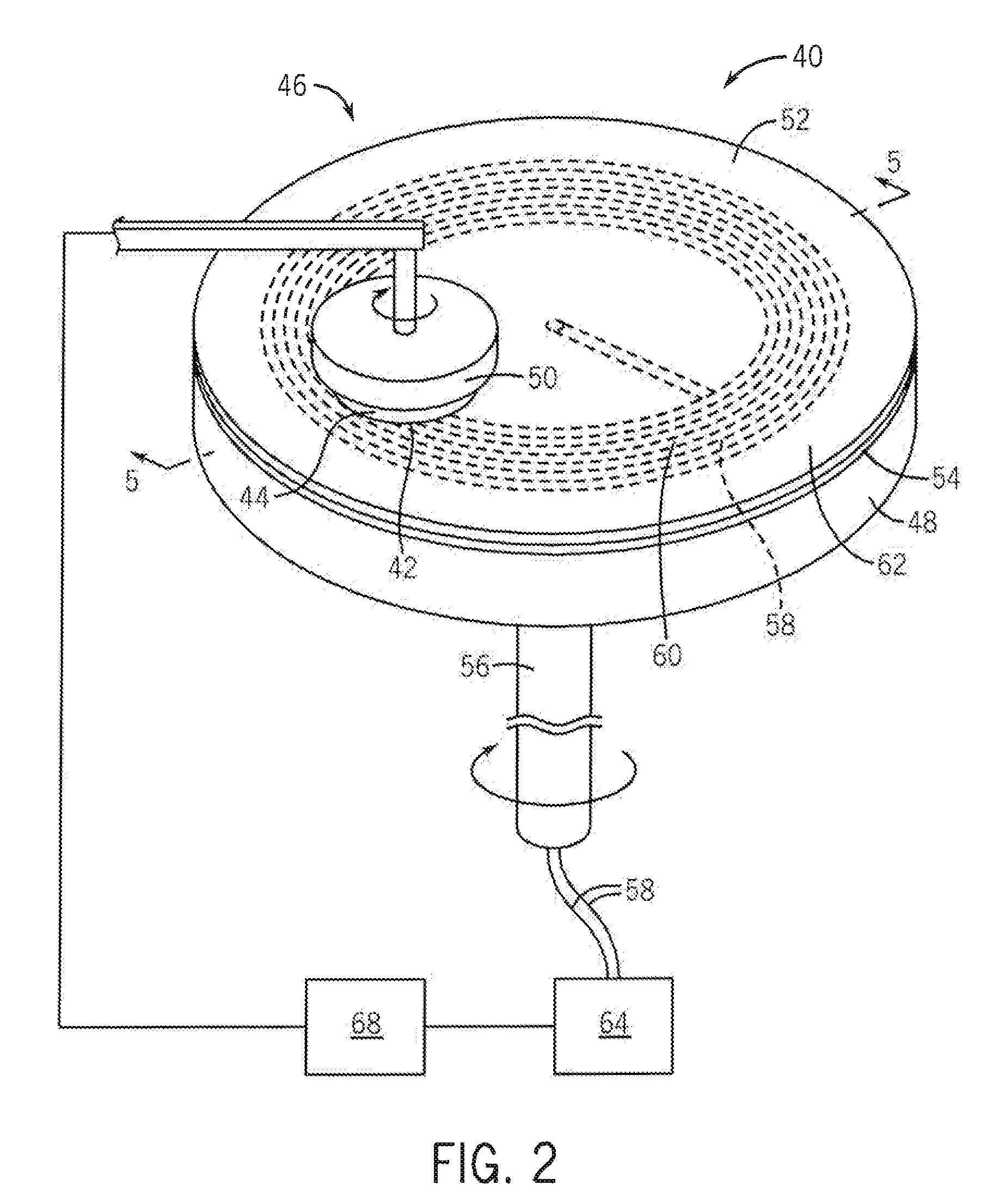
[0032]The following description with reference to the drawings provides illustrative examples of devices, assemblies, systems, and methods for monitoring and / or endpointing planarizing and conditioning processes in mechanical or chemical-mechanical planarization of semiconductor wafers and other microelectronic substrates according to the invention. Such description is for illustrative purposes only and not for purposes of limiting the same. The present invention can be utilized to provide other embodiments of devices, assemblies, and systems in accordance with the invention.

[0033]In the context of the current application, the term “semiconductor substrate” or “semiconductive substrate” or “semiconductive wafer fragment” or “wafer fragment” or “wafer” will be understood to mean any construction comprising semiconductor material, including but not limited to bulk semiconductive materials such as a semiconductor wafer (either alone or in assemblies comprising other materials thereon),...


PUM

PropertyMeasurementUnit
widthaaaaaaaaaa
wavelengthaaaaaaaaaa
vibrational energyaaaaaaaaaa

Abstract

Devices, systems and methods for monitoring characteristics of semiconductor substrates and workpieces during planarization and for endpointing planarization processes are provided. The invention utilizes a fiber optic contact sensor incorporated into a planarizing pad or pad-subpad assembly for process monitoring of mechanical energy (e.g., mechanical vibration) and acoustical energy (e.g., ultrasonic vibration) that allows an operator to determine status and / or an endpoint of a planarizing or polishing process. In another embodiment, the invention utilizes a fiber optic contact sensor incorporated into a table support for a planarizing pad.

Description

FIELD OF THE INVENTION[0001]The invention relates generally to apparatus and methods for endpointing mechanical and / or chemical-mechanical planarization of semiconductor wafers and other microelectronic substrates.BACKGROUND OF THE INVENTION[0002]Fabricating integrated circuit devices involves forming multiple layers of conducting, semiconducting, dielectric, and insulting materials on a substrate. During fabrication, the substrate is typically planarized at various stages to make it level and uniform, and eliminate recesses, protrusions, scratches, and other undesirable topology, which can cause step coverage problems for the deposition of a subsequent material layer and depth of focus problems that impair photolithographic processes used to form sub-micron features.[0003]Chemical-mechanical polishing and chemical-mechanical planarization processes, both of which are referred to herein as “CMP” processes, are abrasive techniques that typically include the use of a combination of ch...

Claims


Application Information

Patent Timeline
Patent Type & Authority Patents(United States)
IPC IPC(8): B24B49/00
CPCB24B37/013B24B37/205B24B49/16
Inventor KISTLER, RODNEY C.
Owner MICRON TECH INC
Why Eureka
Try Eureka