Method for manufacturing SOI substrate

a silicononinsulator and substrate technology, applied in semiconductor/solid-state device manufacturing, basic electric elements, electric devices, etc., can solve the problems of reducing increasing the thickness of the periphery of the buried oxide film, and increasing the thickness of the periphery

Active Publication Date: 2009-05-26
KIOXIA CORP +1
View PDF4 Cites 9 Cited by
  • Summary
  • Abstract
  • Description
  • Claims
  • Application Information

AI Technical Summary

Benefits of technology

[0015]Moreover, in the conventional method described in Patent Document 2, it is known that the periphery of the upper margin of a surface oxide film serving as a mask when oxygen ions are implanted is deformed so as to be expanded. When a part of a surface oxide film is protruded to a portion not covered with the surface oxide film, a fear is presented that the implantation depth of oxygen ions to be implanted may be changed. Therefore, it is also necessary to effectively prevent the edge area of the obtained buried oxide film from being exposed on the surface of a substrate by inhibiting deformation in which a part of the surface oxide film is protruded to a portion not covered with the surface oxide film and uniforming the depth of the buried oxide film when oxygen ions are implanted.
[0049]Furthermore, by forming a recess portion on the upper corner of the mask oxide film, even if the upper margin on the mask oxide film is deformed so as to be extended at the time of oxygen ion implantation, the deformed portion is not protruded to a portion not covered with the mask oxide film and thus the implantation depth of implanted oxygen ions is not changed. Therefore, the thickness of the buried oxide film obtained trough oxygen ion implantation becomes uniform and it is possible to prevent the edge area of the buried oxide film from being exposed on the surface of a substrate.

Problems solved by technology

As a result, a trouble that a step is formed on the surface of the substrate 2 after removing a surface oxide layer 8 occurs.
This deformation presents a fear that when a part of the surface oxide film is protruded to a portion serving as an SOI area not covered with the surface oxide film, a fear is presented that the implantation depth of oxygen ions to be implanted may be changed.
Furthermore, in the above method described in Patent Document 1, there is a problem that the peripheral portion of an oxygen ion area serving as a buried oxide film is more oxidized than the central portion of the oxygen ion area at the time of annealing after implanting oxygen ions and expanded in volume.
When increase in the thickness advances, there is a problem that the peripheral portion is exposed on the surface of the substrate.

Method used


Image

  • Method for manufacturing SOI substrate
  • Method for manufacturing SOI substrate
  • Method for manufacturing SOI substrate

Examples


first embodiment

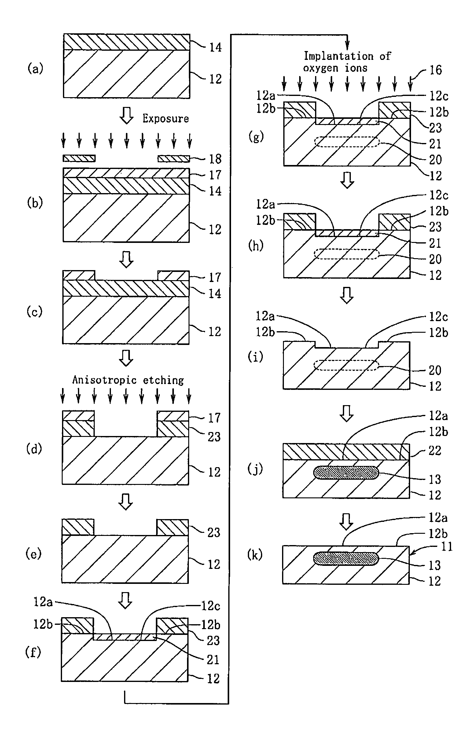
[0062]As shown in FIG. 1(k), an SOI substrate 11 has a silicon substrate 12 and a buried oxide film 13 formed inside the substrate 12. The substrate 12 is cut in a sliced form along a plane perpendicular to the axis of a single-crystal silicon rod grown by Czochralski (CZ) method [plane (100) of a crystal structure of a single crystal silicon]. Moreover, a buried oxide film 13 is formed as described below. It is allowed to cut a substrate from a single-crystal silicon rod or single-crystal silicon plate grown not by the CZ method but by the floating zone (FZ) method or the like.

[0063]Firstly, a surface oxide film 14 is formed on the surface of the substrate 12 (FIG. 1(a)). This surface oxide film 14 is a silicon oxide film (SiO2 film), which is formed by thermally oxidizing the substrate 12 or with the CVD method (chemical vapor deposition method). Moreover, the surface oxide film 14 is formed in the thickness range between 200 and 1,000 nm, preferably in the thickness range between...

second embodiment

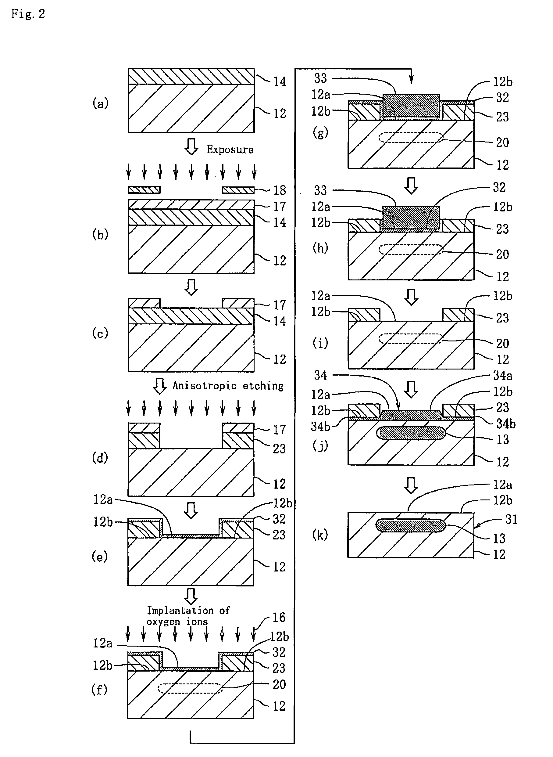
[0069]FIG. 2 shows second embodiment of the present invention. In FIG. 2, a nemeral same as that in FIG. 1 denotes the same component.

[0070]This embodiment further includes a step of forming a buffer film 32 on the substrate surface 12a serving as an SOI area where a mask oxide film 23 is not formed and on the upside and the side of a mask oxide film 23. Specifically, a buffer film 32 made of silicon nitride is formed on the substrate surface 12a serving as an SOI area and the upside and the side of the mask oxide film 23 after vertically anisotropically etching a surface oxide film 14 vertically to the surface of a substrate 12 by using a resist layer 17 as a mask (FIG. 2(d)) before implanting oxygen ions 16 (FIG. 2(f)). The thickness of the buffer film 32 ranges between 5 and 500 nm, preferably between 20 and 200 nm. This limitation of the thickness of the buffer film 32 in the range of 5 to 500 nm because it is impossible to prevent oxygen from entering from a boundary area at th...

third embodiment

[0075]FIG. 3 shows third embodiment of the present invention. In FIG. 3, a numeral same as that in FIG. 1 denotes the same component.

[0076]This embodiment further includes a step of etching a mask oxide film 23 to form a predetermined thickness and a step of forming a buffer film 42 on a predetermined-width boundary area contacting with the side of the mask oxide film 23 of silicon substrate surface 12a serving as an SOI area and on the side of the mask oxide film 23 between a step of implanting oxygen ions 16 and a step of performing annealing. Specifically, after implanting oxygen ions 16 (FIG. 3(e)), the mask oxide film 23 is decreased in thickness so that the difference between thicknesses of the oxide film 34a formed on the substrate surface 12a serving as an SOI area at the time of annealing to be described later and an oxide film 34b to be newly formed on the substrate surface 12b serving as a bulk area (thickness of the oxide film 34a minus thickness of the oxide film 34b) b...


PUM

PropertyMeasurementUnit
thicknessaaaaaaaaaa
thicknessaaaaaaaaaa
thicknessaaaaaaaaaa

Abstract

To easily and accurately flush a substrate surface serving an SOI area with a substrate surface serving as a bulk area, make a buried oxide film, and prevent an oxide film from being exposed on substrate surface. After partially forming a mask oxide film 23 on the surface of a substrate 12 constituted of single crystal silicon, oxygen ions 16 are implanted into the surface of the substrate through the mask oxide film, and the substrate is annealed to form a buried oxide film 13 inside the substrate. Further included is a step of forming a predetermined-depth concave portion 12c deeper than substrate surface 12b serving as a bulk area on which the mask oxide film is formed on the substrate surface 12a serving as an SOI area by forming a thermally grown oxide film 21 on the substrate surface 12a serving as an SOI area on which the mask oxide film is not formed between the step of forming the mask oxide film and the step of implanting oxygen ions.

Description

BACKGROUND OF THE INVENTION[0001]1. Field of the Invention[0002]The present invention relates to a method for manufacturing a Silicon-On-Insulator (SOI) substrate partially having a buried oxide film in a silicon substrate by a Separation by IMplanted Oxygen (SIMOX) method.[0003]2. Description of the Related Art[0004]It is conventionally expected to use an SOI substrate having a buried oxide film in a silicon substrate for high-speed low-power-consumption device substrates. Among these device substrates, an SOI substrate having a buried oxide film in a silicon substrate not entirely but partially (hereafter referred to as “partial SOI substrate”) is regarded to be important because it is possible to form only a logic portion in an SOI area of a buried oxide film in a system LSI including analog logic memories and to manufacture a memory portion at a bulk Si portion without the buried oxide film.[0005]As this type of method for manufacturing the partial SOI substrate (method for manu...

Claims


Application Information

Patent Timeline
Patent Type & Authority Patents(United States)
IPC IPC(8): H01L21/8238
CPCH01L21/76243
Inventor NAKAI, TETSUYAKO, BONG-GYUNHAMAMOTO, TAKESHIYAMADA, TAKASHI
Owner KIOXIA CORP
Why Eureka
Try Eureka