Touch panel and manufacturing method thereof

a technology of touch panel and manufacturing method, which is applied in the field of touch panel, can solve problems such as operation errors in electronic equipment, and achieve the effects of preventing detection errors, reducing manufacturing costs, and simplifying structur

Inactive Publication Date: 2009-05-26
PANASONIC CORP
View PDF8 Cites 9 Cited by
  • Summary
  • Abstract
  • Description
  • Claims
  • Application Information

AI Technical Summary

Benefits of technology

[0012]The present invention is to provide a touch panel with a simplified structure capable of reliable operation free from errors. The touch panel of the present invention includes a top substrate, a top conductive layer, a pair of top electrodes, a bottom substrate, a bottom conductive layer, a pair of bottom electrodes, and a frame-like spacer. The top conductive layer and the top electrodes are provided on the top substrate, and the top electrodes extend from respective both ends of the top conductive layer. The bottom conductive layer and the bottom electrodes are provided on the bottom substrate, and the bottom conductive layer faces the top conductive layer with a prescribed clearance. The bottom electrodes extend from both ends of the bottom conductive layer in a direction perpendicular to the extending direction of the top electrodes. The spacer is formed on the periphery of the top substrate and the bottom substrate therebetween. A first separate area insulated from the top conductive layer and extending in a direction perpendicular to the extending direction of the top electrodes is provided near an inner periphery of the spacer on a surface of the top substrate where the top conductive layer is provided. And / or a second separate area insulated from the bottom conductive layer and extending in a direction perpendicular to an extending direction of the bottom electrode is provided near an inner periphery of the spacer on a surface of the bottom substrate where the bottom conductive layer is provided. In the touch panel, the pressed place will not be detected even in a case that the end of the top substrate is bent by a force applied mistakenly. Despite the simplified structure, therefore, it can prevent detection errors.

Problems solved by technology

Even in the case that the end of top conductive layer 53 contacts with bottom conductive layer due to the reasons described above, the electronic circuit would detect erroneously as if the touch panel is operated to press down, causing an operation error in the electronic equipment.

Method used


Image

  • Touch panel and manufacturing method thereof
  • Touch panel and manufacturing method thereof
  • Touch panel and manufacturing method thereof

Examples


Embodiment Construction

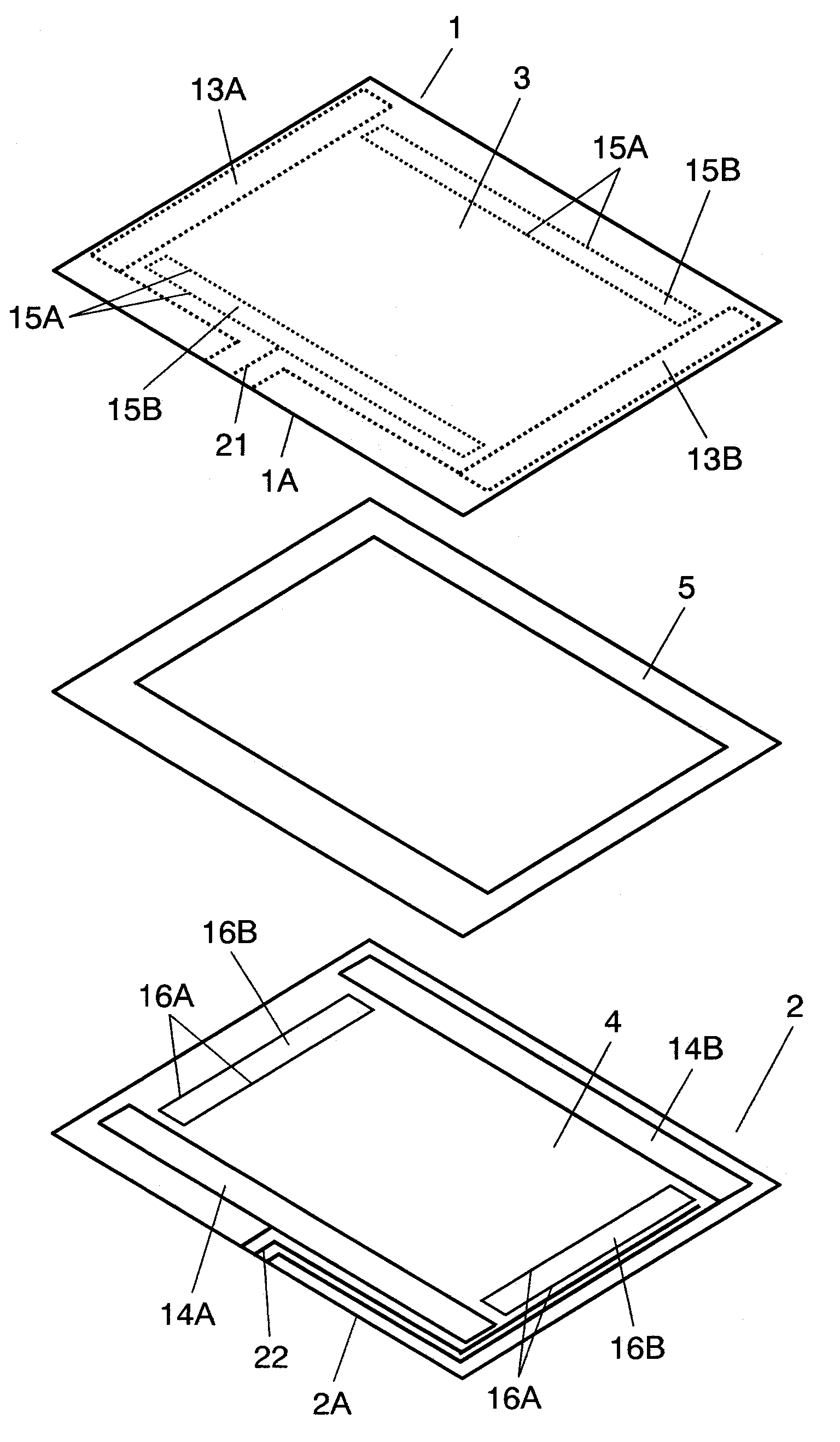
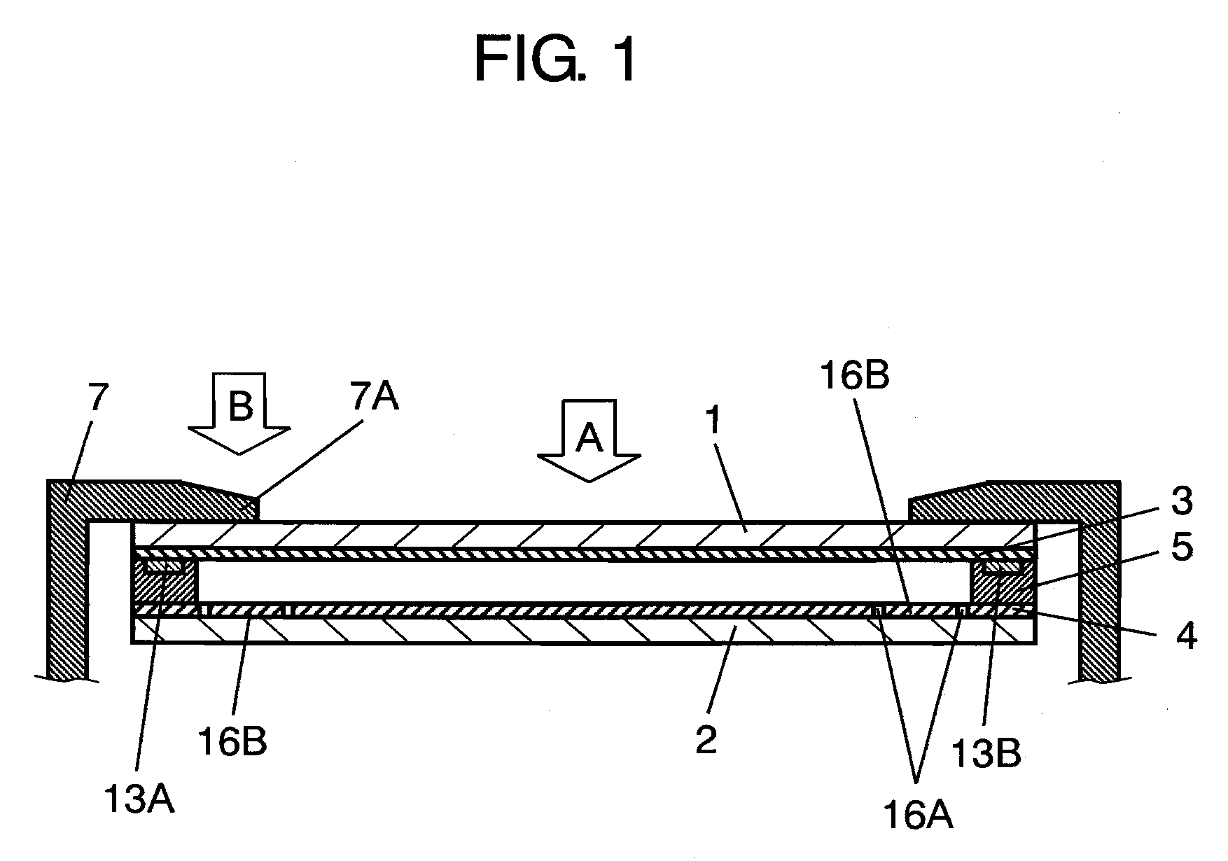
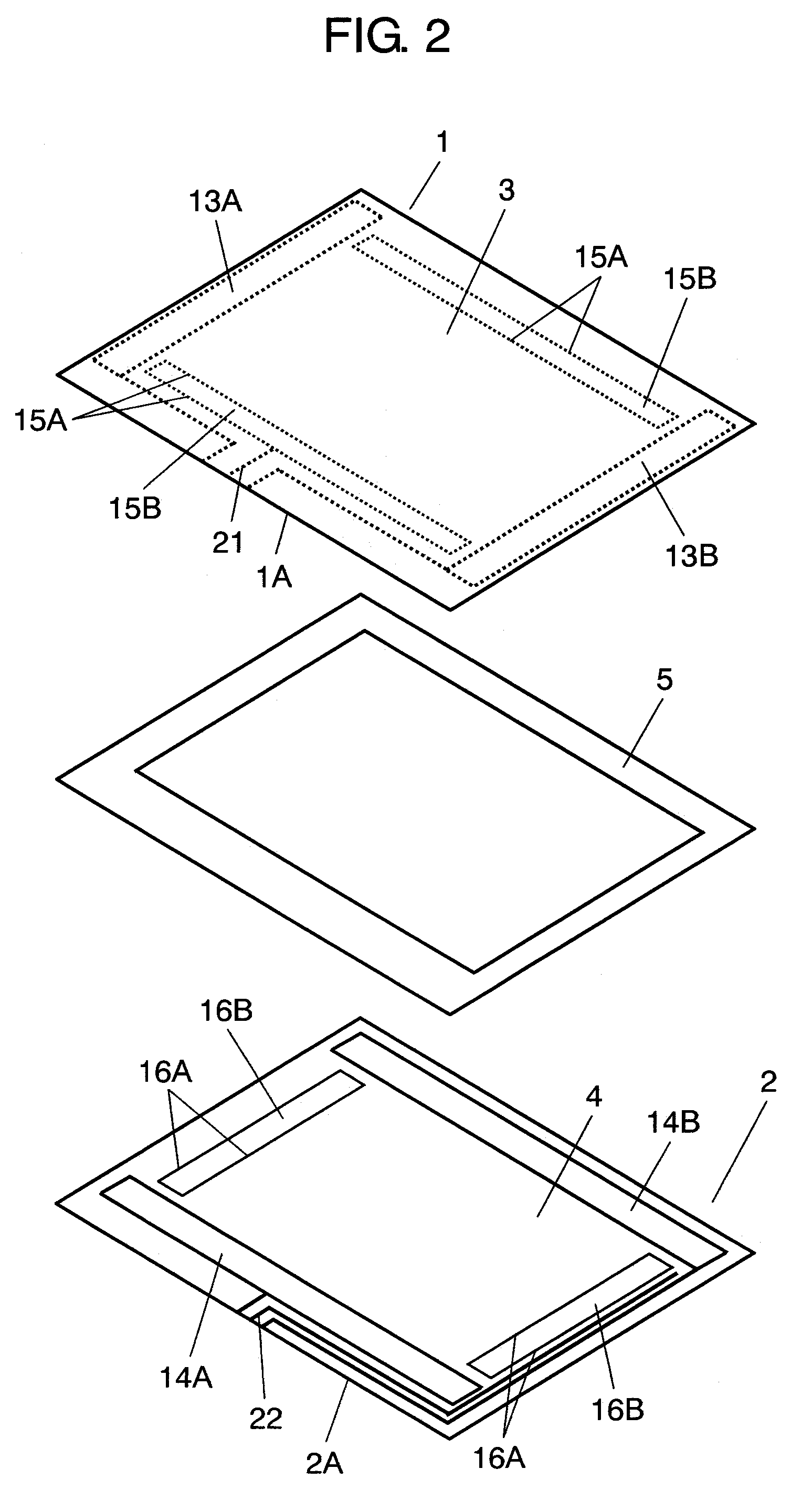
[0016]An exemplary embodiment of the present invention is described with reference to the drawings. A cross-sectional view in the drawings is shown on an expanded scale in a thickness direction so that the configuration can be understood easily.

[0017]FIG. 1 is a cross-sectional view of the touch panel according to an exemplary embodiment of the present invention, and FIG. 2 is an exploded perspective view of the same. The touch panel includes top substrate 1 and bottom substrate 2, both light transparent. Top substrate 1 is made of polyethylene-terephthalate, polycarbonate, glass or the like. Bottom substrate 2 is made of glass, acrylic, polycarbonate or the like. Light transparent top conductive layer 3 made of indium tin oxide or the like is formed on the bottom surface of top substrate 1 by sputtering or the like, and bottom conductive layer 4 is similarly formed on the top surface of bottom substrate 2.

[0018]Dot spacers (not shown) made of insulating resin such as epoxy resin an...


PUM

PropertyMeasurementUnit
conductiveaaaaaaaaaa
areaaaaaaaaaaa
thicknessaaaaaaaaaa

Abstract

A first separate area insulated from a top conductive layer and extending in a direction perpendicular to an extending direction of top electrodes is provided near an inner periphery of a spacer on a surface of the top substrate where the top conductive layer is provided. And / or a second separate area insulated from a bottom conductive layer and extending in a direction perpendicular to an extending direction of bottom electrodes is provided near an inner periphery of the spacer on a surface of the bottom substrate where the bottom conductive layer is provided.

Description

BACKGROUND OF THE INVENTION[0001]1. Field of the Invention[0002]The present invention relates to a touch panel mainly used to operate a wide variety of electronic equipment and a manufacturing method thereof.[0003]2. Background Art[0004]In recent years, a wide variety of electronic equipment such as mobile phones and car navigation systems has advanced in functions and become diversified. Along with this, equipment like following is increasing in number. That is, to select respective functions of the equipment, a user operates to press down a touch panel by a finger, a pen or the like while viewing a display element such as a liquid crystal display (LCD) device through a light transparent touch panel. The touch panel is attached on the front surface of the display element. Such equipment requires having a highly visible touch panel with reliable operability.[0005]A conventional touch panel of this kind is described with reference to FIG. 3. FIG. 3 shows a cross-sectional view of a c...

Claims


Application Information

Patent Timeline
Patent Type & Authority Patents(United States)
IPC IPC(8): H01H1/10
CPCG06F3/045H01H13/702Y10T29/49105H01H2211/036H01H2219/01H01H2211/024
Inventor FUJII, SHIGEYUKINAKANISHI, AKIRA
Owner PANASONIC CORP
Why Eureka
Try Eureka