Reversible electric fuse and antifuse structures for semiconductor devices

a technology of electronic fuse and antifuse, which is applied in the direction of semiconductor devices, semiconductor/solid-state device details, electrical apparatus, etc., can solve the problems of material migration, further current crowing, and complicated design of electronic fuse, so as to facilitate the second electromigration, facilitate the reversibility of electric current flow, and increase the electrical conductivity

Active Publication Date: 2009-07-07
GLOBALFOUNDRIES U S INC
View PDF15 Cites 75 Cited by
  • Summary
  • Abstract
  • Description
  • Claims
  • Application Information

AI Technical Summary

Benefits of technology

[0015]In another embodiment, a method of forming an integrated circuit having a fuse and antifuse structure is described, the method including depositing a first and a second material layer on a semiconductor substrate, wherein the second material layer having a higher electrical conductivity than the first material layer; selectively etching the first and second material layer to create at least one constricted region to facilitate electromigration of the second material; wherein the electromigration creates a plurality of micro voids; and forming a plurality of electrical contacts on the second material layer. In this particular embodiment, the first material is selected from a group consisting of Ta, TaN, TiN, Ru, RuN, W and WN; the second material is selected from a group consisting of Cu, Ru, Ir, Rh and Pt; and the electrical contacts include a material selected from a group consisting of Cu, Al, W, TiN, TaN, Ta, and Mo. In addition, the micro voids are configured for facilitating reversibility of an electric current flow.

Problems solved by technology

However, because the laser beam is relatively large, this technique requires enough clearance between the fuse element and the rest of the circuitry to avoid collateral damage.
Current crowding takes place around a fixed location thus initiating electromigration which results in further current crowing and material migration along the direction of the electron movement along the fuse element.
However, the design of an electronic fuse is more complicated, particularly in the choice of the material and the integration scheme employed.

Method used


Image

  • Reversible electric fuse and antifuse structures for semiconductor devices
  • Reversible electric fuse and antifuse structures for semiconductor devices
  • Reversible electric fuse and antifuse structures for semiconductor devices

Examples


Embodiment Construction

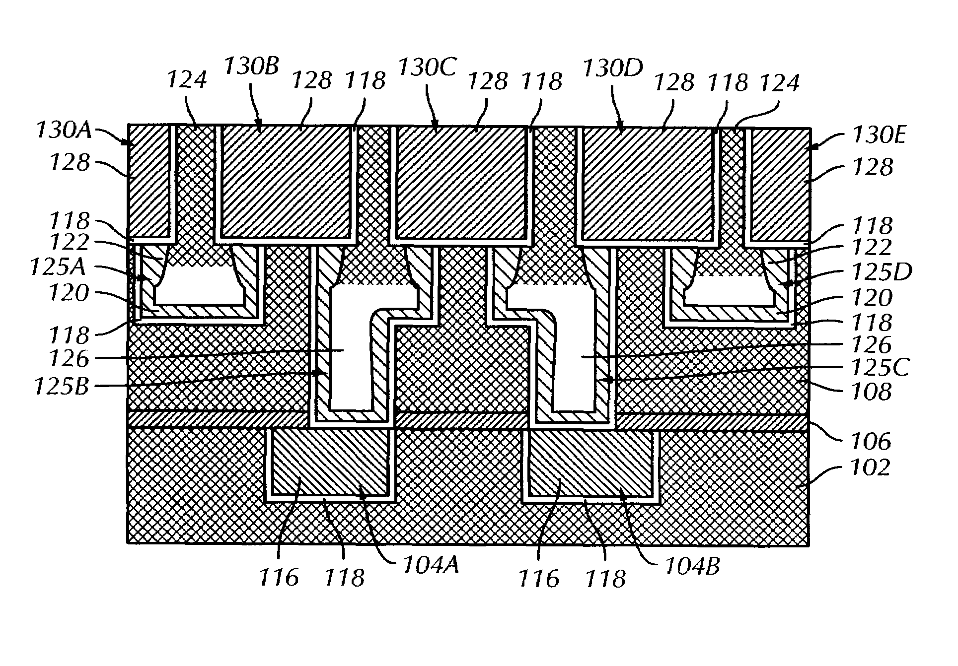
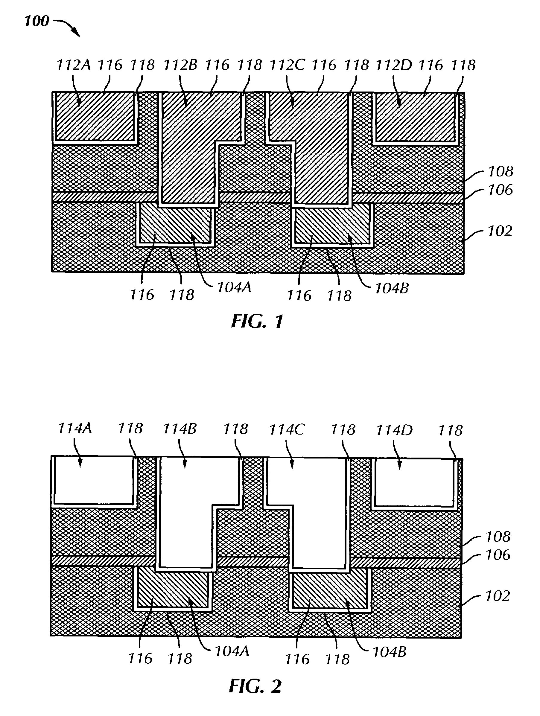
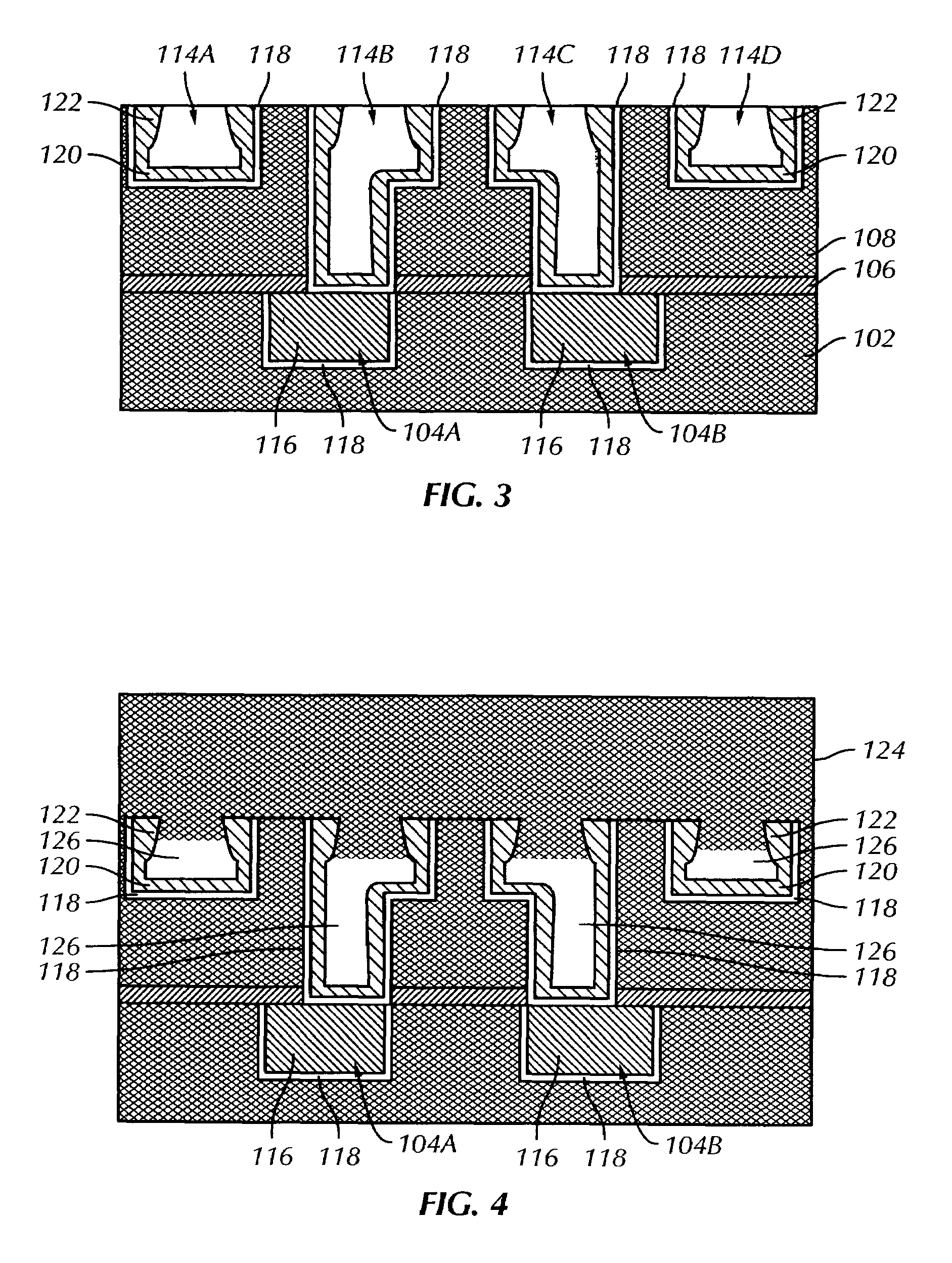
[0034]Referring now to the drawing figures, wherein like references numerals identify identical or corresponding elements throughout the several views, an embodiment of the presently disclosed structure and method of forming fuse and antifuse structures will now be disclosed in detail. In the following description, numerous specific details are set forth, such as particular structures, components, materials, dimensions, processing steps and techniques, in order to provide a thorough understanding of the present invention. However, it will be appreciated by one skilled in the art that the invention may be practiced without these specific details. In other instances, well-known structures or processing steps have not been described in detail to avoid obscuring the invention. The materials described herein are employed to illustrate the present disclosure in one application and should not be construed as limiting.

[0035]It will be understood that when a layer is referred to as being “on...


PUM


Abstract

A structure and method of fabricating reversible fuse and antifuse structures for semiconductor devices is provided. In one embodiment, the method includes forming at least one line having a via opening for exposing a portion of a plurality of interconnect features; conformally depositing a first material layer over the via opening; depositing a second material layer over the first material layer, wherein the depositing overhangs a portion of the second material layer on a top portion of the via opening; and depositing a blanket layer of insulating material, where the depositing forms a plurality of fuse elements each having an airgap between the insulating material and the second material layer. The method further includes forming a plurality of electroplates in the insulator material connecting the fuse elements. In another embodiment, the method includes depositing a first and a second material layer on a semiconductor substrate, wherein the second material layer having a higher electrical conductivity than the first material layer; selectively etching the first and second material layer to create at least one constricted region to facilitate electromigration of the second material; wherein the electromigration creates a plurality of micro voids; and forming a plurality of electrical contacts on the second material layer.

Description

BACKGROUND OF THE INVENTION[0001]1. Technical Field[0002]The present disclosure relates generally to integrated circuit semiconductor devices. In particular, the present disclosure relates to reversible electronic fuse and antifuse structures for semiconductor devices.[0003]2. Description of Related Art[0004]The proliferation of electronics in our modern world is in large part due to integrated circuit semiconductor devices. Integrated semiconductor devices are designed and used in widely differing applications and there are currently numerous schemes for providing integrated circuit interconnections well known in the art, for example, electrically programmable interconnections for use in integrated circuits. Electrically programmable interconnect schemes include fuses and antifuse devices. Fuses are reprogrammable interconnect, which may be altered by a user after initial circuit configuration has been accomplished. Antifuses are one-time programmable, that is, it cannot be reconfi...

Claims


Application Information

Patent Timeline
Patent Type & Authority Patents(United States)
IPC IPC(8): H01L23/58
CPCH01L23/5252H01L23/5256H01L28/24H01L2924/0002H01L2924/00
Inventor WONG, KEITH KWONG HONYANG, CHIH-CHAOYANG, HAINING S
Owner GLOBALFOUNDRIES U S INC
Why Eureka
Try Eureka