Chip for light-emitting diode and preparation method thereof

A technology of light-emitting diodes and chips, applied in electrical components, circuits, semiconductor devices, etc., can solve problems such as low reliability and easy breakage, and achieve the effects of improving reliability, enhancing stability, and avoiding electrode breakage.

Inactive Publication Date: 2017-09-12
HC SEMITEK ZHEJIANG CO LTD
View PDF6 Cites 0 Cited by
  • Summary
  • Abstract
  • Description
  • Claims
  • Application Information

AI Technical Summary

Problems solved by technology

[0006] In order to solve the problem that the electrodes in the prior art are easy to break when used for a long time and cause the reliability of the LED to be low, the embodiment of the present invention provides a light-emitting diode chip and its preparation method

Method used


Image

  • Chip for light-emitting diode and preparation method thereof
  • Chip for light-emitting diode and preparation method thereof
  • Chip for light-emitting diode and preparation method thereof

Examples


Embodiment 1

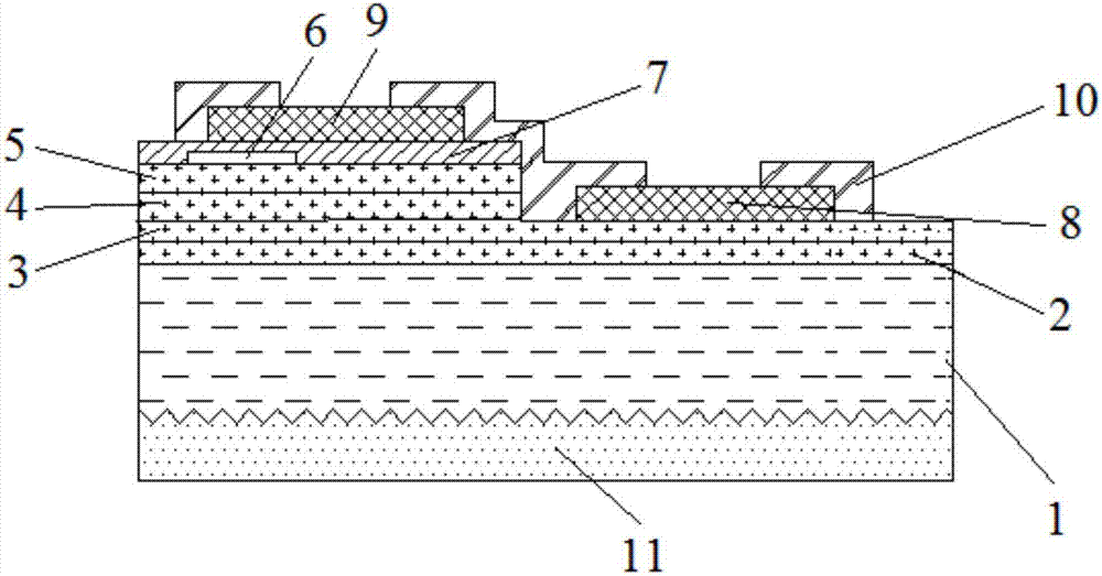
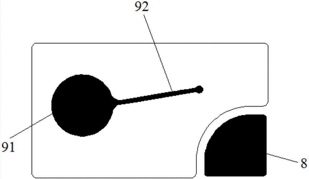
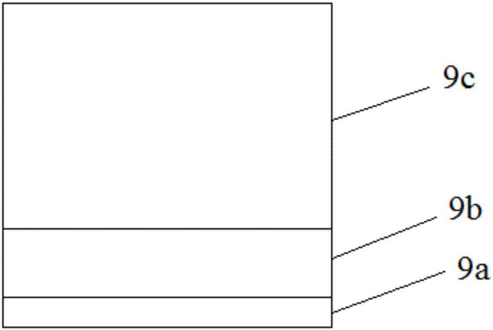
[0036] An embodiment of the present invention provides a light emitting diode chip, see figure 1 , the chip includes a substrate 1, and a gallium nitride buffer layer 2, an n-type gallium nitride layer 3, a multi-quantum well layer 4, a p-type gallium nitride layer 5, and a current blocking layer 6 stacked on the substrate 1 in sequence and a transparent conductive layer 7 , the chip is provided with grooves extending from the transparent conductive layer 7 to the N-type gallium nitride layer 3 . The chip also includes an N-type electrode 8, a P-type electrode 9 and a passivation layer 10. The N-type electrode 8 is arranged on the N-type gallium nitride layer 3 in the groove, and the passivation layer 10 is arranged on the transparent conductive layer 7, the concave On the sidewall of the groove and on the N-type gallium nitride layer 3 in the groove. The P-type electrode includes a cylinder whose bottom surface is arranged on the P-type gallium nitride layer and the transpar...

Embodiment 2

[0054] The embodiment of the present invention provides a method for preparing a light-emitting diode chip, which is suitable for preparing the chip provided in Embodiment 1, see Figure 4 , the preparation method comprises:

[0055] Step 201: sequentially growing a GaN buffer layer, an N-type GaN layer, a multi-quantum well layer, and a P-type GaN layer on the substrate.

[0056] Specifically, the substrate is a sapphire substrate. The multi-quantum well layer may include multiple indium gallium nitride layers and multiple gallium nitride layers, and the multiple indium gallium nitride layers and multiple gallium nitride layers are alternately stacked.

[0057] Step 202: Open a groove extending from the P-type GaN layer to the N-type GaN layer.

[0058] Step 203: forming a current blocking layer and a transparent conductive layer on the P-type GaN layer.

[0059] Specifically, the material of the current blocking layer may be silicon dioxide or aluminum oxide, and the thic...


PUM

PropertyMeasurementUnit
thicknessaaaaaaaaaa
thicknessaaaaaaaaaa
thicknessaaaaaaaaaa

Abstract

The present invention disclosed a chip and preparation method of glowing diodes, which are semiconductor technology.The chip includes substrate, nitride buffer layer, N -type nitride layer, multi -quantum trap layer, P type nitride layer, current blocking layer, transparent conductive layer, N -type electrode, P -type electrode and passivation layer;The N -type electrode is set on the N -type nitride layer in the groove, and the passivation layer is set on the N -type nitride layer in the transparent conductive layer, the side wall of the groove and the groove;The cylindrical body on the P -type nitride layer and the transparent conductive layer and the strip body set on the transparent conductive layer at least one bottom surface is extended from the side of the cylindrical body.Om contact layer, reflective layer, and welded layer, the material of the reflector is aluminum -silicon copper alloy, the mass score of the silicon in aluminum silicon copper alloy is 1 % to 2 %, the mass score of copper in aluminum silicon copper alloy is 0.5 % ~ 1%.The invention improves chip reliability.

Description

technical field [0001] The invention relates to the technical field of semiconductors, in particular to a chip of a light emitting diode and a preparation method thereof. Background technique [0002] Light Emitting Diode (English: Light Emitting Diode, referred to as: LED) is a semiconductor light emitting device made by using the principle of semiconductor PN junction electroluminescence. LED is a green and environment-friendly lighting source. There are no ultraviolet and infrared rays in the spectrum. There is neither heat nor harmful radiation in the emitted light, and the waste can be recycled. In addition, LED also has the advantages of low voltage, low power consumption, small size, light weight, etc., and can be made into various forms of products such as points, lines, and surfaces. At the same time, the control is extremely convenient, and the light intensity can be adjusted at will by adjusting the current. The use of timing control circuit can achieve rich and ...

Claims


Application Information

Patent Timeline
Patent Type & Authority Applications(China)
IPC IPC(8): H01L33/00H01L33/06H01L33/60
CPCH01L33/60H01L33/0075H01L33/06
Inventor 兰叶顾小云黄龙杰杨春艳吴志浩王江波
Owner HC SEMITEK ZHEJIANG CO LTD
Why Eureka
Try Eureka