Electromigration resistant metal layer structure and process method thereof
A process method and metal layer technology, applied in circuits, electrical components, electrical solid devices, etc., can solve the problems that metal AL is prone to electromigration, etc., and achieve the effect of improving the anti-electromigration ability
- Summary
- Abstract
- Description
- Claims
- Application Information
AI Technical Summary
Problems solved by technology
Method used
Image
Examples
Embodiment 1
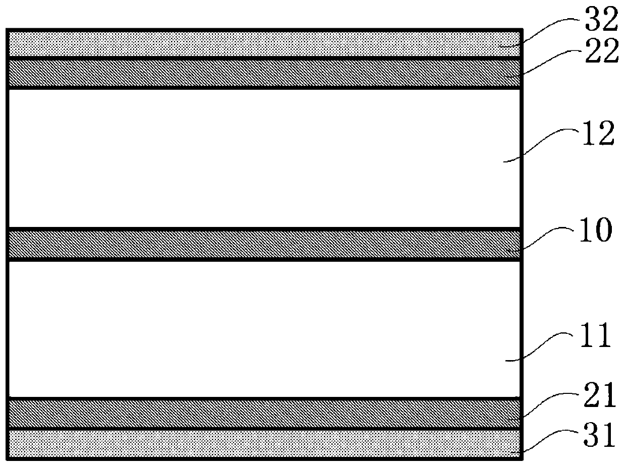
[0025] Embodiment 1 of the present invention provides an anti-electromigration metal layer structure, which is an anti-electromigration structure for a metal layer in back-end manufacturing. The structure of the anti-electromigration metal layer structure is as follows figure 1 As shown, it includes two aluminum layers, for the convenience of description, the two aluminum layers are respectively represented as the first aluminum layer 11 and the second aluminum layer 12; and, the first aluminum layer 11 and the second aluminum layer The thickness of 12 is 2000~3000Å, and the thinner thickness of the aluminum layer helps to limit the boundary diffusion of large grains. A central TiN layer 10 is deposited between the first aluminum layer 11 and the second aluminum layer 12; wherein, the thickness of the central TiN layer 10 is 50-150 Å, as the first aluminum layer 11 and the The barrier layer of the second aluminum layer 12.
[0026] Specifically, a first TiN layer 21 and a fi...
Embodiment 2
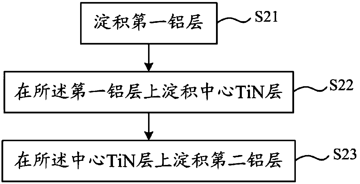
[0028] Embodiment 2 of the present invention provides a process method for an anti-electromigration metal layer structure, and its schematic flow chart is as follows figure 2 shown. Described processing method comprises the steps:
[0029] S21, depositing a first aluminum layer;
[0030] S22. Depositing a central TiN layer on the first aluminum layer;
[0031] S23, depositing a second aluminum layer on the central TiN layer.
[0032] Specifically, firstly, the first Ti layer 31 and the first TiN layer 21 are sequentially deposited on the insulating dielectric layer, and the first Al layer 11 is deposited on the first TiN layer 21 . A central TiN layer 10 is deposited on the first aluminum layer 11 , and the thickness of the central TiN layer 10 is 50˜150 Å; a second aluminum layer 12 is deposited on the central TiN layer 10 . Finally, a second TiN layer 22 and a second Ti layer 32 are sequentially deposited on the second aluminum layer 12 .
[0033] Preferably, copper is...
PUM
 Abstract
Description
Claims
Application Information

