Semiconductor structure and formation method thereof

A semiconductor and gas technology, applied in semiconductor devices, semiconductor/solid-state device manufacturing, semiconductor/solid-state device components, etc., can solve the problems that the electrical performance of semiconductor structures needs to be improved, so as to improve electrical performance and reliability, and optimize electrical performance , Improve the effect of electrical performance

Active Publication Date: 2016-02-17
SEMICON MFG INT (SHANGHAI) CORP
View PDF7 Cites 6 Cited by
  • Summary
  • Abstract
  • Description
  • Claims
  • Application Information

AI Technical Summary

Problems solved by technology

[0006] However, the electrical performance of existing semiconductor structures formed by TSV technology needs to be improved

Method used


Image

  • Semiconductor structure and formation method thereof
  • Semiconductor structure and formation method thereof
  • Semiconductor structure and formation method thereof

Examples


Embodiment Construction

[0039] It can be seen from the background art that the electrical performance of the semiconductor structure formed in the prior art is relatively poor.

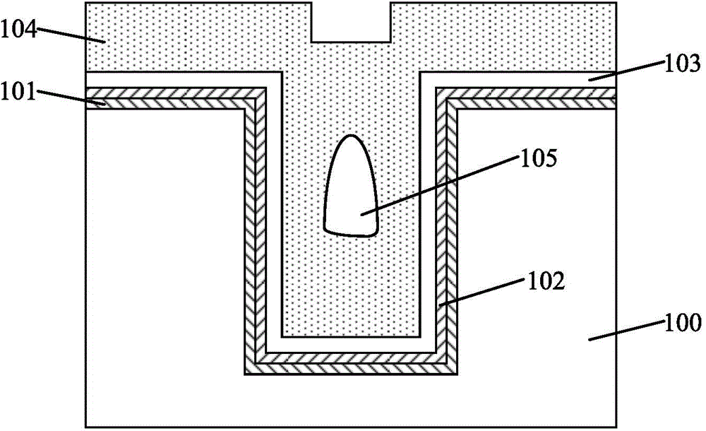
[0040] Conduct research on the formation method of the semiconductor structure, the formation method of the semiconductor structure includes the following steps, please refer to figure 1 , figure 1 A schematic cross-sectional structure of a semiconductor structure, providing a substrate 100 with a through hole; forming an oxide layer 101 on the bottom and sidewall surfaces of the through hole 100 and the top surface of the substrate 100; forming a barrier layer 102 on the surface of the oxide layer 101 ; forming a seed layer 103 on the surface of the barrier layer 102 ; forming a metal body layer 104 on the surface of the seed layer 103 , and the metal body layer 104 fills the through hole.

[0041] Since Cu has lower resistivity, higher melting point and lower thermal expansion coefficient than Al, Cu is generally used as ...


PUM

PropertyMeasurementUnit
thicknessaaaaaaaaaa
thicknessaaaaaaaaaa
thicknessaaaaaaaaaa

Abstract

A semiconductor structure and a formation method thereof are disclosed. The formation method of the semiconductor structure comprises the following steps of providing a substrate and forming a through hole in the substrate; forming amorphous silicon layers on a through hole bottom and a sidewall surface; forming a barrier layer on an amorphous silicon layer surface, wherein the barrier layer preferentially orients a crystal plane (111); and forming a metal layer on a barrier layer surface, wherein the metal layer fills in the through hole and the metal layer preferentially orients the crystal plane (111). In the invention, after the amorphous silicon layers are formed on the silicon through hole bottom and the sidewall surface, the barrier layer and the metal layer which preferentially orient the crystal plane (111) are formed on the amorphous silicon layer surface so that an electromigration resistance capability of the metal layer is increased; a resistance of the metal layer is reduced; an electromigration resistance capability of the semiconductor structure is increased; an RC delayed effect of the semiconductor structure is reduced and electric performance of the semiconductor structure is improved.

Description

technical field [0001] The invention relates to the technology in the field of semiconductor manufacturing, in particular to a semiconductor structure and a method for forming the same. Background technique [0002] With the rapid development of semiconductor manufacturing technology, in order to achieve faster computing speed, larger data storage capacity and more functions, semiconductor chips are developing towards higher integration. The higher the integration degree of the semiconductor chip, the smaller the characteristic size (CD: Critical Dimension) of the semiconductor device. [0003] A three-dimensional integrated circuit (IC: Integrated Circuit) is manufactured using advanced chip stacking technology, which is to stack chips with different functions into an integrated circuit with a three-dimensional structure. Compared with two-dimensional integrated circuits, the stacking technology of three-dimensional integrated circuits can not only shorten the signal trans...

Claims


Application Information

Patent Timeline
Patent Type & Authority Applications(China)
IPC IPC(8): H01L21/768H01L23/48
CPCH01L21/0243H01L21/02488H01L21/76843H01L21/76873H01L2924/0002H01L23/481H01L21/76898H01L21/02532H01L21/0262H01L2924/00H01L21/76802H01L21/30625H01L21/76831
Inventor 何作鹏赵洪波
Owner SEMICON MFG INT (SHANGHAI) CORP
Why Eureka
Try Eureka