Electromigration resistant interconnect structure

a technology of electromigration resistance and metal interconnect, which is applied in the direction of semiconductor devices, semiconductor/solid-state device details, electrical apparatus, etc., can solve the problems of metal ions to dislodge from the lattice and move physically, metal line or metal via no longer providing a conductive path in the metal interconnect, and product failure of semiconductor devices, etc., to achieve the effect of reducing parasitic resistance and increasing the electromigration resistance of the metal lin

Inactive Publication Date: 2009-02-12
IBM CORP
View PDF8 Cites 7 Cited by
  • Summary
  • Abstract
  • Description
  • Claims
  • Application Information

AI Technical Summary

Benefits of technology

[0015]A line trench is formed in a dielectric layer that may contain an interlayer dielectric material. A metal liner is formed on the sidewalls and the bottom surface of the line trench. A conductive metal is deposited within a remaining portion of the line trench at least up to a top surface of the dielectric layer and planarized to form a metal line in the line trench. The metal line is recessed by a recess etch below the top surface of the dielectric layer. A dielectric line cap or a metallic line cap is formed by deposition of a dielectric cap layer or a metallic cap layer, followed by planarization of the dielectric or metallic cap layer. The dielectric line cap or the metallic line cap applies a highly compressive stress on the underlying metal line, which increases electromigration resistance of the metal line. The dielectric line cap or the metal line cap does not extend laterally outside the region immediately above the metal line, resulting in a reduced parasitic resistance compared with prior art metal interconnect structures.

Problems solved by technology

High defect density, i.e., smaller grain size of the metal, or high temperature typically increases electron scattering, and consequently, the amount of momentum transfer from the electrons to the conductor material.
Such momentum transfer, if performed sufficiently cumulatively, may cause the metal ions to dislodge from the lattice and move physically.
Such a void results in a locally increased resistance in the metal interconnect, or even an outright circuit “open.” In this case, the metal line or the metal via no longer provides a conductive path in the metal interconnect.
Formation of voids in the metal line or the metal via can thus result in a product failure in semiconductor devices.
Such void, if formed in a semiconductor device, may cause a circuit failure, and possibly, a device failure.
As feature sizes of semiconductor devices continue to shrink, current density through metal interconnect structures increase, causing the metal interconnect structures to be more prone to electromigration failure.
Such electromigration failure increases the frequency of product failure over a lifetime of semiconductor devices, and consequently, degrades reliability of the semiconductor devices.

Method used


Image

  • Electromigration resistant interconnect structure
  • Electromigration resistant interconnect structure
  • Electromigration resistant interconnect structure

Examples


first embodiment

[0059]Referring to FIG. 3, a first exemplary metal interconnect structure according to the present invention comprises a dielectric layer 10 containing a line trench LT, or a trench formed along a line. The sidewalls of the line trench LT may be substantially vertical, or may have an inward taper so that the bottom surface of the line trench LT is narrower than the opening at the top portion of the line trench LT. The taper angle may be from 0 degree to about 30 degrees, and typically from about 5 degrees to about 20 degrees, depending on the material of the dielectric layer 10, the width of the opening at the top portion of the line trench LT, the etch chemistry employed in etching the line trench LT, and the depth of the line trench LT.

[0060]The dielectric layer 10 may comprise an oxide based conventional dielectric material, which has a dielectric constant k from about 3.6 to about 3.9, or a low-k dielectric material, which has a dielectric constant k of about 3.0 or less, prefer...

second embodiment

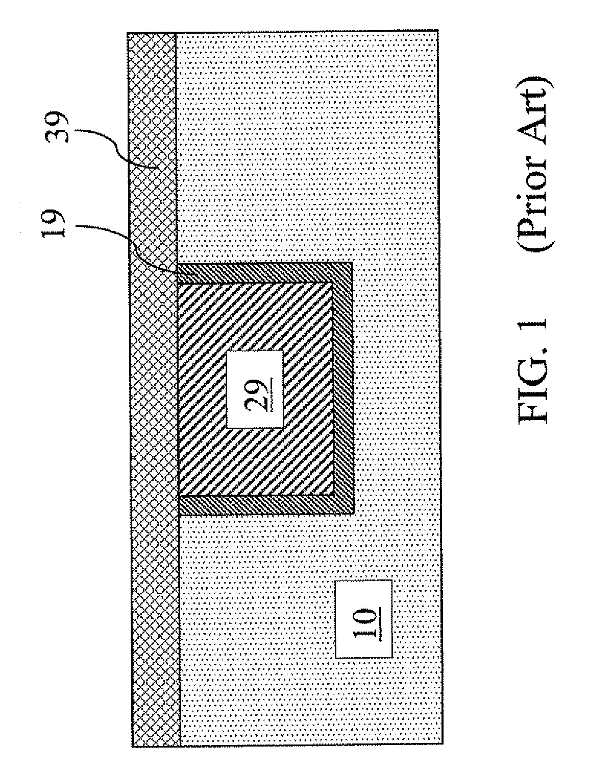
[0074]Referring to FIG. 12, a second exemplary metal interconnect structure according to the present invention is derived from the first exemplary metal interconnect structure of FIG. 7 by depositing a metallic line cap layer 49 on the metal line top surface 31, a top portion of inner sidewalls of the metal liner 20, and the dielectric layer top surface 11. Preferably, the thickness of the metallic line cap layer 49 is at least equal to the recess depth d, and may be from about 5 nm to about 100 nm, and preferably from about 12 nm to about 50 nm, although lesser and greater thicknesses are herein contemplated also.

[0075]The metallic line cap layer 49 comprises a stress-generating material that may apply a compressive stress on a structure directly underneath. For example, the metallic line cap liner 39 may comprise one of Ti, TiN, Ta, TaN, WN, and CoWP. The metallic line cap liner 39 may, or may not, comprise the same material as the metal line 20. The metallic line cap liner 39 may...


PUM

PropertyMeasurementUnit
compressive stressaaaaaaaaaa

Abstract

A line trench is formed in a dielectric layer that may contain an interlayer dielectric material. A metal liner is formed on the sidewalls and the bottom surface of the line trench. A conductive metal is deposited within a remaining portion of the line trench at least up to a top surface of the dielectric layer and planarized to form a metal line in the line trench. The metal line is recessed by a recess etch below the top surface of the dielectric layer. A dielectric line cap or a metallic line cap is formed by deposition of a dielectric cap layer or a metallic cap layer, followed by planarization of the dielectric or metallic cap layer. The dielectric line cap or the metallic line cap applies a highly compressive stress on the underlying metal line, which increases electromigration resistance of the metal line.

Description

FIELD OF THE INVENTION[0001]The present invention relates to semiconductor structures, and particularly to electromigration resistant metal interconnect structures and methods of manufacturing thereof.BACKGROUND OF THE INVENTION[0002]A metal line comprises a lattice of metal ions and non-localized free electrons. The metal ions are formed from metal atoms that donate some of their electrons to a common conduction band of the lattice, and the non-localized free electrons move with relatively small resistance within the lattice under an electric field. Normal metal lines, excluding superconducting materials at or below a superconducting temperature, have finite conductivity, which is caused by interaction of electrons with crystalline imperfections and phonons which are thermally induced lattice vibrations.[0003]When electrical current flows in the metal line, the metal ions are subjected to an electrostatic force due to the charge of the metal ion and the electric field to which the ...

Claims


Application Information

Patent Timeline
Patent Type & Authority Applications(United States)
IPC IPC(8): H01L23/52H01L21/4763
CPCH01L21/76834H01L21/76883H01L21/76849
Inventor YANG, HAINING S.YANG, CHIH-CHAOWONG, KEITH KWONG HON
Owner IBM CORP
Why Eureka
Try Eureka