Embedded electroconductive layer structure

Inactive Publication Date: 2005-05-10
FUJITSU SEMICON LTD
View PDF27 Cites 5 Cited by
  • Summary
  • Abstract
  • Description
  • Claims
  • Application Information

AI Technical Summary

Benefits of technology

[0058]Thirdly, a combined supply of a metal complex of Cu with a metal compound of Al is available. This supply permits formatio

Problems solved by technology

Cu, however, encounters the problem that the conventional RIE (reactive ion etching) technique fails to afford an ample etching rate at low temperatures because a halogenide of Cu has a low vapor pressure.
It also has the problem of rendering anisotropic etching difficult.
Further, Cu easily diffuses in SiO2, forms a deep sublevel in a silicon semiconductor, and curtails the service life of minority carriers.
The growth of the Cu layer under discussion, therefore, encounters the problem that the CVD-TiN layer does not function as a barrier metal.
When a TiN

Method used


Image

  • Embedded electroconductive layer structure
  • Embedded electroconductive layer structure
  • Embedded electroconductive layer structure

Examples


first embodiment

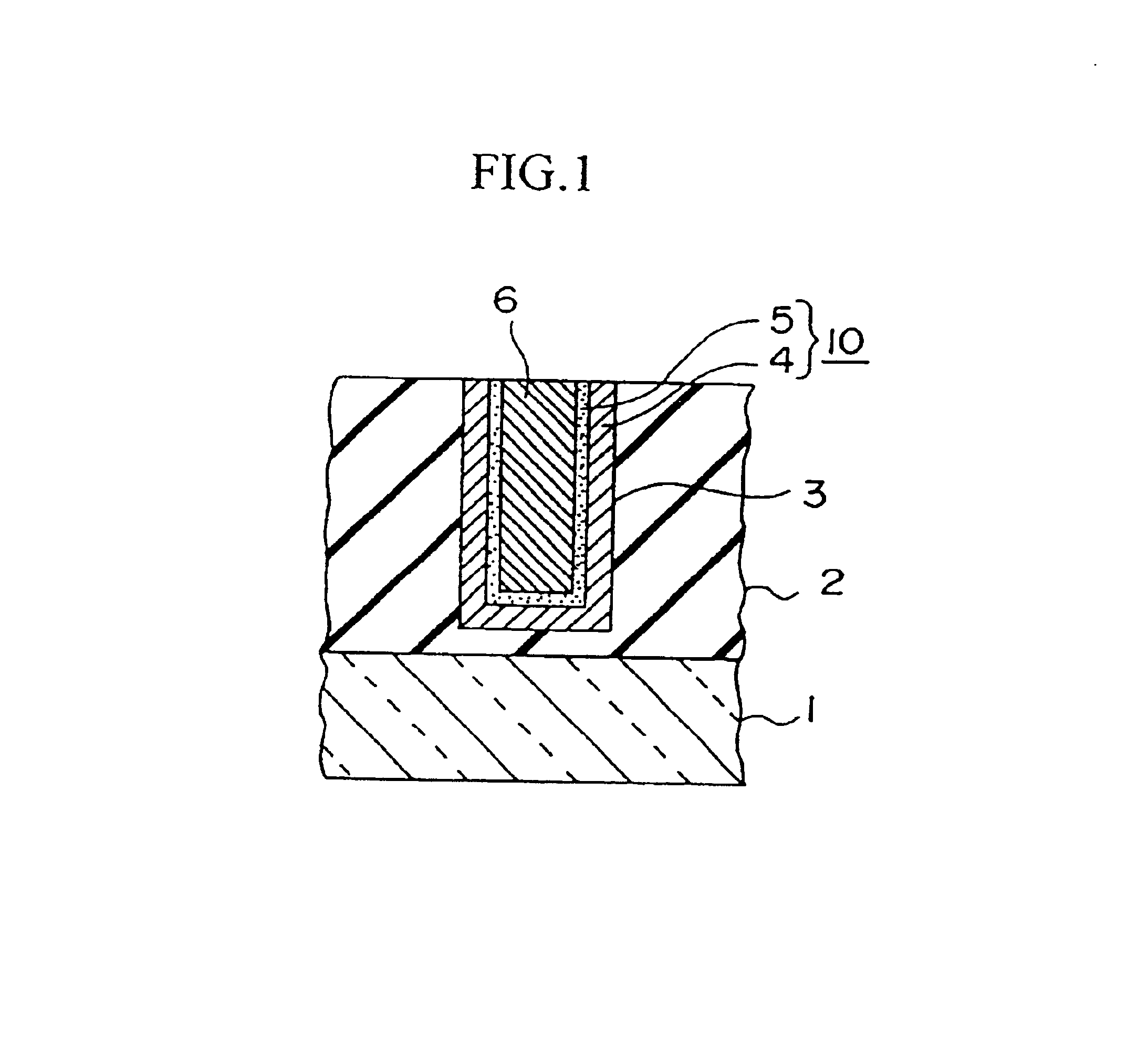
[0074]The first embodiment of this invention will be described below with reference to FIGS. 7A to 7E. The reaction devices which are mentioned in the embodiments of this invention are assumed to have inner volumes of 40-80 liters.

[0075]First, an SiO, layer 12 is deposited in a thickness of 600 nm by the plasma CVD method on a silicon substrate 11 having a 6-inch (about 15 cm) (100) plane 6 as a main surface thereof, a photoresist is applied thereon in a thickness of 0.6 μm and then the SiO2 layer 12 is covered with a mask of photoresist pattern formed in advance through the steps of exposure and patterning and etched along a wiring pattern by the use of an i ray (365 nm) to form a groove 13 of a width of 300 nm and a depth of 500 nm as shown in FIG. 7A.

[0076]In this case, a TEOS (tetra-ethyl-orthosilicate)-SiO2 layer, an SOG (spin-on glass) layer, or a PSG (phosphosilicate glass) layer may be used for the SiO2 layer 12. Otherwise, the SiO2 layer 12 may be formed by thermally oxidiz...

second embodiment

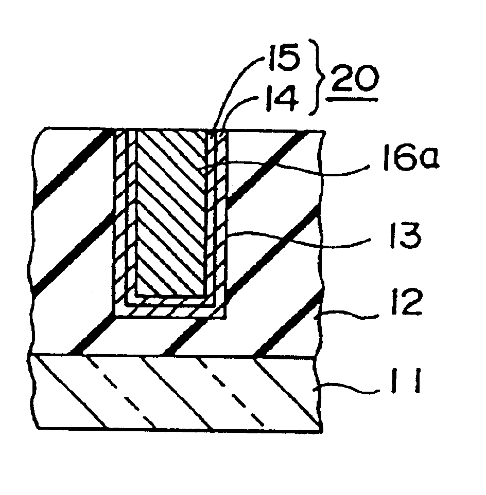
[0085]Now, the second embodiment of this invention will be described below with reference to FIG. 8A and FIG. 8B.

[0086]First. In the same manner as in the first embodiment, the groove 13 for wire distribution is formed in a width of 300 nm and a depth of 500 nm in the SiO2 layer 12 deposited in a thickness of 600 run on the silicon substrate 11 and a WNX layer 14a (x =0 to 1) of a thickness in the range of 10 to 30 nm, preferably 30 nm, is deposited thereon as a barrier layer by the RF sputtering method as shown in FIG. 8A.

[0087]A TaNx, layer (x =0 to 1) may be used in the place of the WN, layer 14a (x =0 to 1). This film exhibits a perfect barrier property to Cu even at such a high temperature as 800° C. (Oku et al., Collection of Manuscripts for Lectures, 30p-K-10, published at the 42nd Joint Lecture Meeting of Physicists Societies held in the spring of 1995).

[0088]Then, in the same manner as in the first embodiment, the CVD-TIN layer 15 of a thickness of 20 nm is deposited by the...

third embodiment

[0090]Now, the third embodiment of this invention will be described below with reference to FIG. 9A to FIG. 9C.

[0091]First, in the same manner as in the first embodiment, the groove 13 destined to encase a interconnection layer therein is formed in the SiO2 layer 12 deposited in a thickness of 600 nm on the silicon substrate 11 as shown in FIG. 9A. The groove 13 has a width of 300 nm and a depth of 500 nm. Subsequently, A PVD-TIN layer 14b Is deposited in a thickness in the range of 10 to 30 nm, preferably in a thickness of 30 nm, by the magnetron sputtering method.

[0092]Then, the PVD-TiN layer 14b is oxidized to form a TiN layer 14c having an oxidized surface as shown in FIG. 9B. N2 gas is supplied at a flow volume in the range of 20000 to 30000 sccm, preferably at a flow volume of 30000 sccm, and the substrate temperature is kept in the range of 400 to 500° C., preferably at 450° C. In the ambience of N2, the layer is annealed for a period in the range of 20 to 60 minutes, prefera...


PUM

PropertyMeasurementUnit
Concentrationaaaaaaaaaa
Electrical conductoraaaaaaaaaa

Abstract

An embedded electroconductive layer is disclosed which comprises an opening part or a depressed part 3 formed in an insulating film 2 on a substrate 1, a barrier layer for covering the opening part or the depressed part, a metal growth promoting layer 5 on the barrier layer, and an electroconductive layer 6 embedded in the opening part or the depressed part via the barrier layer 4 and the metal growth promoting layer 5.

Description

[0001]This is divisional, of application Ser. No. 08 / 959,763, filed Oct. 29, 1997 U.S. Pat. No. 6,090,702 which in turn is a divisional of Ser. No. 08 / 660,524 (U.S. Pat. No. 5,736,192) filed Jun. 7, 1996.BACKGROUND OF THE INVENTION[0002]1. Field of the Invention[0003]This invention relates to an embedded electroconductive layer and a method for the formation thereof. It relates more particularly to an embedded interconnection layer using Cu and Al or a connecting layer (plug) for joining an upper and a lower interconnection layer and a method for the formation thereof.[0004]2. Description of the Prior Art[0005]For the purpose of lowering the resistance offered by an interconnection layer, the feasibility of substituting a Cu interconnection layer for the conventional Al interconnection layer has been the subject of a diligent study. Cu has lower resistivity than Al and about twice as high electromigration resistance as Al.[0006]Generally, the formation of a layer of fine wiring line...

Claims


Application Information

Patent Timeline
IPC IPC(8): C23C16/18H01L23/522H01L23/52H01L21/70H01L23/532H01L21/768C23C14/06C23C14/58C23C16/34
CPCC23C14/0641C23C14/5853C23C16/18C23C16/34H01L21/76846H01L21/76856H01L21/76864H01L21/76877H01L23/5226H01L23/53238H01L2924/0002H01L2924/00
Inventor OKAMOTO, SHIGERU
Owner FUJITSU SEMICON LTD
Why Eureka
Try Eureka