Electro-optical device and electronic apparatus

a technology of optical devices and electronic devices, applied in optics, instruments, printed circuit aspects, etc., can solve the problems of easy crosstalk and difficulty in ensuring that the insulation between the wiring lines is sufficient, and achieve the effect of reliably insulate adjacent source lines or adjacent gate lines, increase the density of wiring lines, and reliably insulate adjacent wiring lines

Active Publication Date: 2009-07-28
BOE TECH GRP CO LTD
View PDF8 Cites 5 Cited by
  • Summary
  • Abstract
  • Description
  • Claims
  • Application Information

AI Technical Summary

Benefits of technology

[0009]An advantage of the invention is that it provides an electro-optical device and an electronic apparatus capable of reliably insulating adjacent wiring lines from each other even when a display panel has a higher definition thereby increasing the wiring line density.
[0010]According to an aspect of the invention, an electro-optical device includes a substrate having a display region; and an extending region extending from the display region. The extending region is provided with wiring lines, and at least some wiring lines, which are disposed to be adjacent to each other, are correspondingly disposed in a plurality of different layers.
[0011]According to the above-mentioned structure of the invention, in the extending region where two substrates do not overlap each other, one substrate being located at the display side and the other substrate being located at the bottom side, it is possible to reliably insulate adjacent source lines or adjacent gate lines from each other, even though the pitch between the adjacent source lines or the adjacent gate lines should be as narrow as possible.
[0012]Further, in the invention, it is preferable that the wiring lines be signal lines.
[0013]According to the above-mentioned structure of the invention, since the number of signal lines, such as a gate line or a source line, increases to make the pitch between the signal lines narrow as the display panel has a higher definition, signal lines adjacent to each other are disposed in two layers, thereby being able to effectively insulate the signal lines from each other.
[0014]In addition, when the signals lines except power lines are closely disposed, crosstalk is apt to occur. Even in this case, by disposing the signal lines adjacent to each other in two layers, the insulation between the layers can be further sufficiently ensured or the distance between the signal lines can increase, which is effective to prevent crosstalk between the signal lines from occurring.

Problems solved by technology

However, the display panel has a problem in that, as the display panel in the electro-optical device has a higher definition, the distance between the wiring lines becomes narrower, so that it becomes difficult to ensure that the insulation between the wiring lines is sufficient.
In addition, when the signals lines except power lines are closely disposed, crosstalk is apt to occur.

Method used


Image

  • Electro-optical device and electronic apparatus
  • Electro-optical device and electronic apparatus
  • Electro-optical device and electronic apparatus

Examples


first embodiment

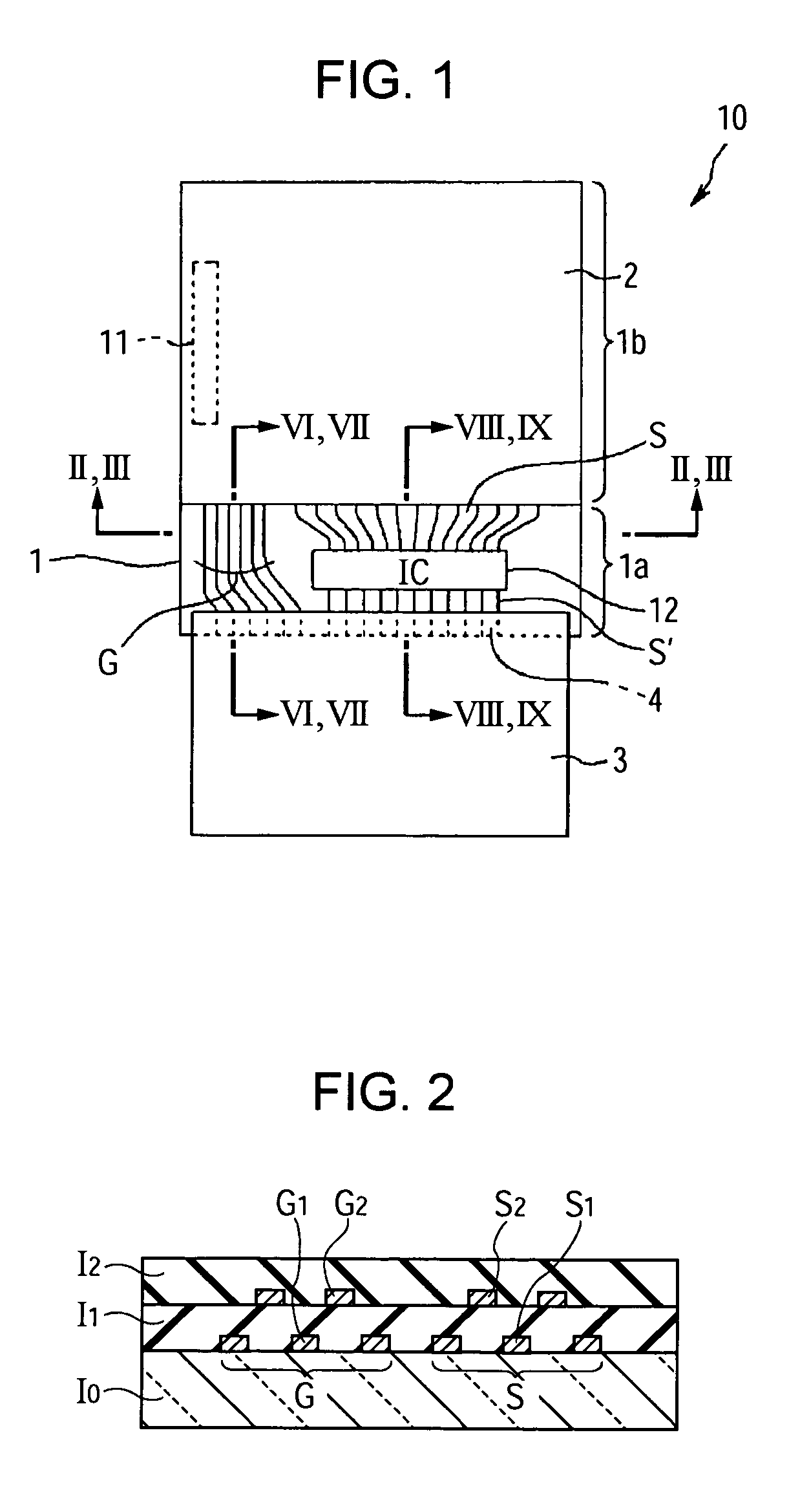
[0039]FIG. 1 is a plan view schematically illustrating an electro-optical device according to a first embodiment of the invention. In the first embodiment, the electro-optical device will be described by using a liquid crystal display device as an example.

[0040]The liquid crystal display device includes a thin film transistor (TFT) active-matrix-type liquid crystal display device, a TFT passive-matrix-type liquid crystal display device, a thin film diode (TFD) active-matrix-type liquid crystal display device, or the like.

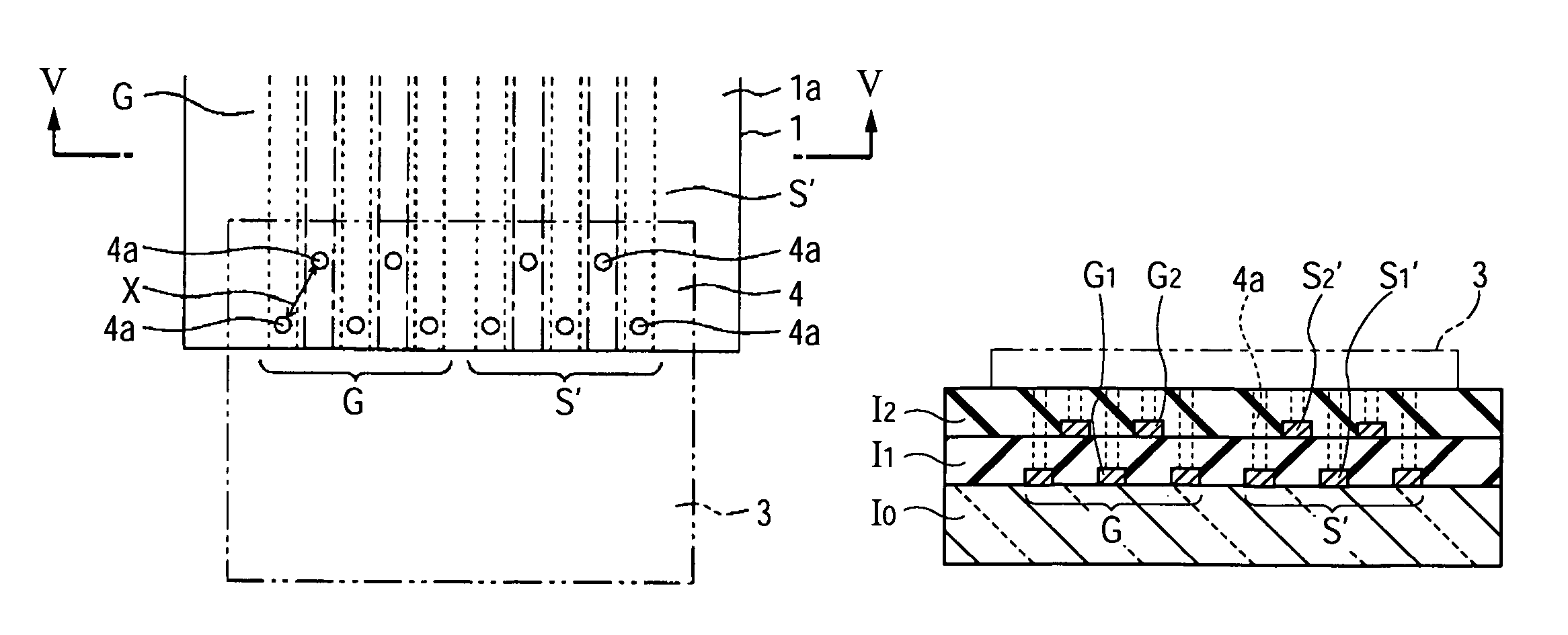
[0041]Referring to FIG. 1, a liquid crystal display device 10 includes a TFT array substrate 1, a counter substrate 2, and a flexible printed board 3 electrically connected to wiring lines in an extending region 1a of the TFT array substrate 1.

[0042]The TFT array substrate 1 has an insulating substrate formed of an insulating member, such as glass. Further, on the TFT array substrate 1, TFTs or gate lines G and source lines S and S′ of the respective TFTs are formed...

second embodiment

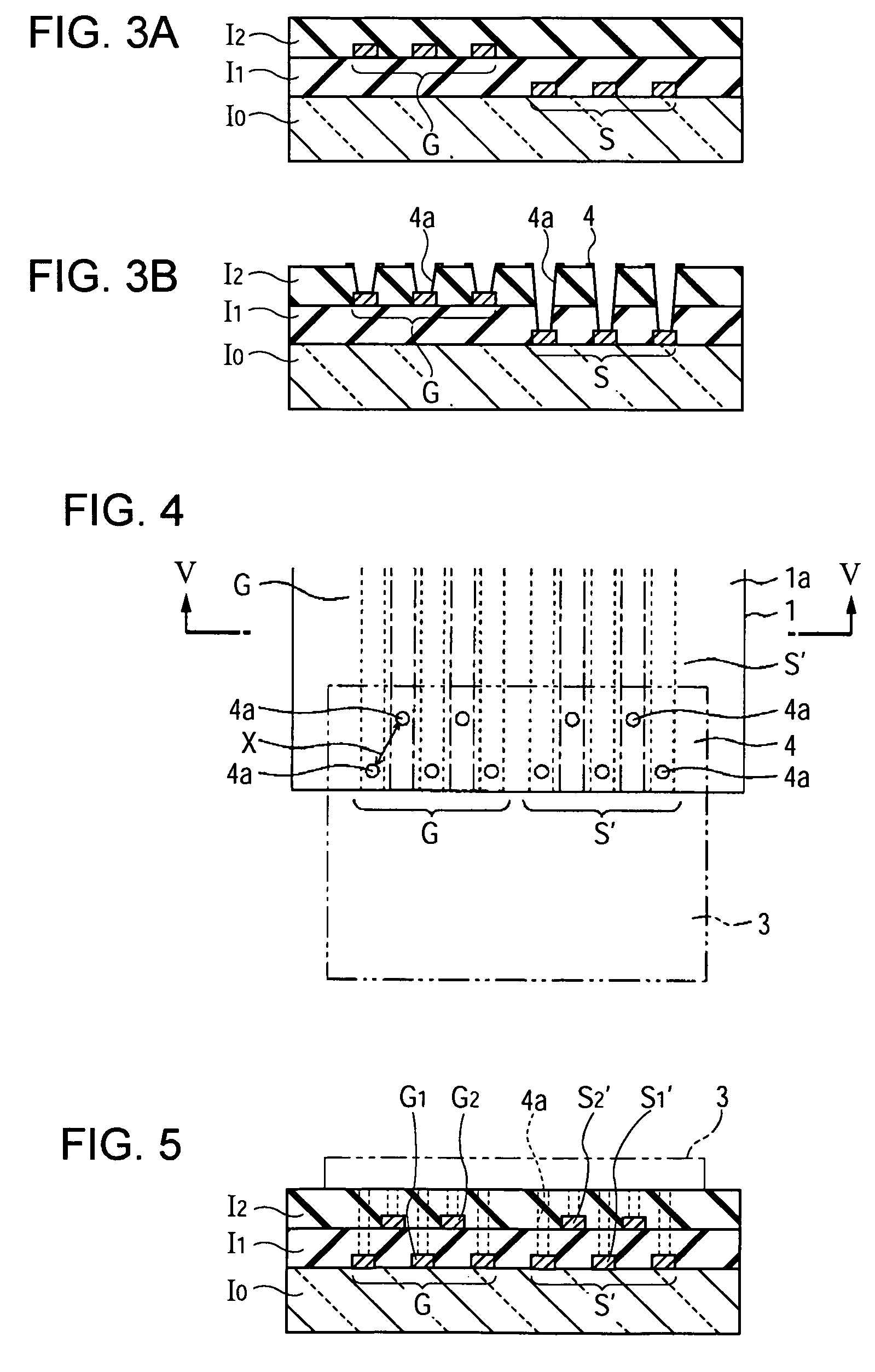
[0055]Next, a second embodiment of the invention will be described through a case in which adjacent wiring lines are disposed in a two-layer structure as in the first embodiment, but overlap each other in an up and down direction.

[0056]FIG. 10 is an enlarged plan view illustrating some of the gate lines and some of the input-side wiring lines of the source driver 12 in the extending region 1a of FIG. 1, according to the second embodiment of the invention. In addition, FIG. 11 illustrates a cross-sectional view taken along the line XI-XI of FIG. 10.

[0057]As shown in FIG. 11, the gate line G1 in the first insulating layer I1 and the gate line G2 in the second insulating layer I2 are disposed to overlap in the up and down direction (that is, in a vertical direction), and the gate line G1′ in the first insulating layer I1 and the gate line G2′ in the second insulating layer I2 are disposed to overlap in the up and down direction. As such, although they are disposed to overlap each other...

third embodiment

[0060]FIG. 12 is a cross-sectional view illustrating a three-layer structure of output-side wiring lines of the source driver 12 and the gate lines in the extending region 1a of FIG. 1, according to a third embodiment of the invention.

[0061]Referring to FIG. 12, a gate line G1 and a source line S1 are formed on the insulating substrate I0 (e.g., glass substrate) constituting the TFT array substrate 1, a first insulating layer I1 is formed thereon, a gate line G2 and a source line S2 are formed on the first insulating layer I1, a second insulating layer I2 is formed thereon, and a gate line G3 and a source line S3 are formed on the second insulating layer I2, and a third insulating layer I3 is formed thereon.

[0062]According to the third embodiment, adjacent gate lines G are formed alternately among the first, second, and third insulating layers I1, I2, and I3, respectively, and adjacent source lines S at the output side of the source driver 12 are also formed alternately among the fi...


PUM

PropertyMeasurementUnit
areaaaaaaaaaaa
conductiveaaaaaaaaaa
resistanceaaaaaaaaaa

Abstract

An electro-optical device includes a substrate having a display region; and an extending region extending from the display region. The extending region is provided with wiring lines, and at least some wiring lines, which are disposed to be adjacent to each other, are correspondingly disposed in a plurality of different layers.

Description

[0001]This application claims priority to Japanese Patent Application No. 2004-253838 filed Sep. 1, 2004 which is hereby expressly incorporated by reference herein in its entirety.BACKGROUND OF THE INVENTION[0002]1. Technical Field[0003]The present invention relates to an electro-optical device and to an electronic apparatus using the same. In particular, the invention relates to an electro-optical device in which adjacent wiring lines, among wiring lines which deliver power and signals required to drive a display panel, can be reliably insulated from each other in an extending region which does not overlap a counter substrate on an insulating substrate, in a display panel structure having an electro-optical material, such as liquid crystal, between the insulating substrate and the counter substrate, and to an electronic apparatus using the same.[0004]2. Related Art[0005]In an electro-optical device, such as a liquid crystal display device, an electroluminescent (EL) device, and a p...

Claims


Application Information

Patent Timeline
Patent Type & Authority Patents(United States)
IPC IPC(8): G02F1/1345
CPCG02F1/13452G02F1/13454G02F1/13458H05K3/361H05K1/117H05K2201/09709H05K3/4644H05K2201/09481H05K2201/09509H01L2224/16225H01L2924/15192G02F1/1345
Inventor YAMADA, KAZUYUKIARUGA, YASUHITO
Owner BOE TECH GRP CO LTD
Why Eureka
Try Eureka