Hot-carrier device degradation modeling and extraction methodologies

a technology of hot-carrier devices and degradation models, applied in the direction of testing circuits, pulse techniques, instruments, etc., can solve the problems of pmos transistor b>10/b> suffering degradation due to device aging, oxide/silicon interface above channel region damage, etc., and achieve the effect of improving accuracy

Active Publication Date: 2009-07-28
CADENCE DESIGN SYST INC
View PDF24 Cites 42 Cited by
  • Summary
  • Abstract
  • Description
  • Claims
  • Application Information

AI Technical Summary

Benefits of technology

[0019]The present invention is directed to a number of improvements in methods for hot-carrier device degradation modeling and extraction. According to a first aspect, several improvements are presented for the improvement of building device degradation models. The user can select the device parameter used to build the device degradation model and the selected device parameter is used to extract device degradation model parameters that will be used for general device parameter degradation. The user can also select the functional relation between stress time and degradation level. In some cases it may be unnecessary to extract voltage acceleration parameters. To further improve accuracy, improved values for one or more acceleration parameters can be extracted again. The use of multiple acceleration parameters can be used to account for different regions of the degradation process.

Problems solved by technology

The design of such circuits is extremely complicated and usually employs simulators, such as SPICE, to predict circuit operation.
With operation over time, the PMOS transistor 10 will suffer degradation due to device aging.
Additionally, the oxide / silicon interface above channel region is damaged by the more energetic holes and electrons.
These effects degrade the transistor's operation in several ways.
The strength of these effects depend differently on bias conditions, but traditionally the change due to lower mobility has been smaller; however, as device sizes have decreased, this interface damage becomes more significant and, depending upon bias conditions, often becomes the larger effect below a quarter micron or so.
These problems are aggravated as device sizes decrease into the submicron region.
These hot electron effects build up over time causing the device to degrade as it ages.
However, the same aged model card can no longer be used for all of the similar devices.
As a real circuit will often contain thousands or even millions of elements, the simulation of the aging of such circuits is a extremely complicated process for which a large number of improvements are desirable.

Method used


Image

  • Hot-carrier device degradation modeling and extraction methodologies
  • Hot-carrier device degradation modeling and extraction methodologies
  • Hot-carrier device degradation modeling and extraction methodologies

Examples


first embodiment

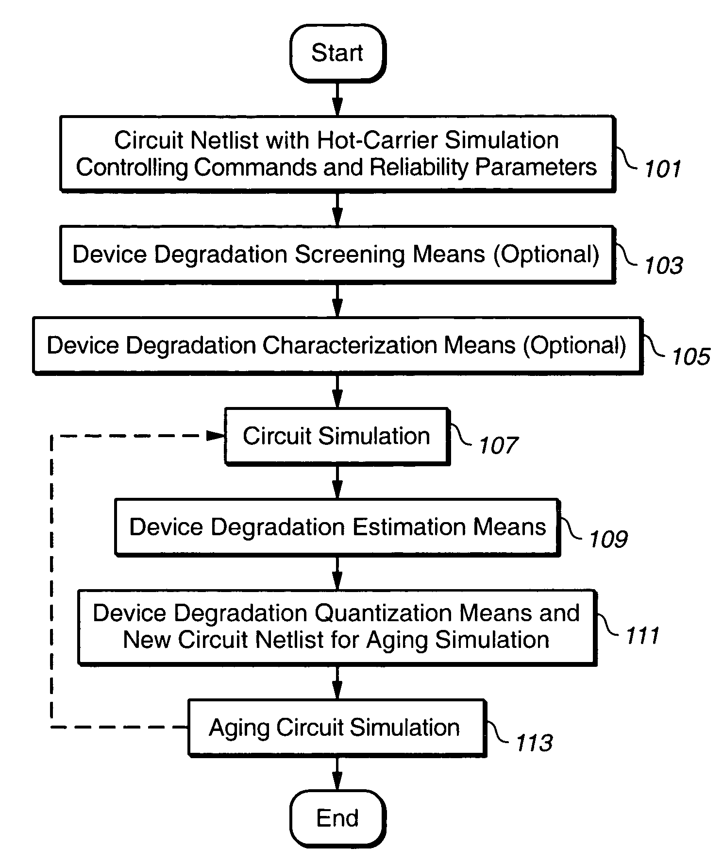
[0105]FIG. 11 is a flow chart of the first embodiment for building degraded device model. At step 1101, the devices will be stressed, and device characteristics and parameters will be measured at several time intervals. This can be performed at the same time as step 901 above, but makes additional measurements. In step 901, points were obtained for parameters at the time values; here, curves such as the I-V characteristics at the time values are also measured as these are used to extract the SPICE or other model. Step 1103 builds the device degradation model from the measured device parameters. This is the flow of FIG. 9 above.

[0106]In step 1105, fresh and degraded device models are built from the measured device characteristics and the device degradation level is calculated for each device model. The fresh and degraded models can be built separately. The model cards are extracted from the respective fresh and degraded curves, such as those shown in FIG. 12. FIG. 12 shows Ids−Vds cu...

second embodiment

[0109]FIG. 14 is a flow chart of a second embodiment for building degraded device model. Referring to FIG. 14, at step 1401, devices will be stressed, device characteristics and parameters will be measured at several time intervals. At step 1403, build device age model from measured device parameters. These are the same as in steps 1101 and 1103

[0110]The second embodiment differs in the next pair of steps. At step 1405, fresh device models are again built from measured device characteristics and device ages are again calculated for the stressed devices. Unlike step 1105, it is only the fresh models, and not the degraded models, that are constructed. The age is calculated from the Age=(AR)t relation.

[0111]At step 1407, analytical functions can be used to build the aged device model parameters as a function of device age by fitting the measured device parameters vs. device age values. Device model parameter at any age value can be calculated from the function. With this analytical fun...


PUM


Abstract

The present invention is directed to a number of improvements in methods for hot-carrier device degradation modeling and extraction. Several improvements are presented for the improvement of building device degradation models, including allowing the user to select a device parameter used to build the device degradation model independent of the device parameter selected. The user can also select the functional relation between stress time and degradation level. To further improve accuracy, multiple acceleration parameters can be used to account for different regions of the degradation process. Analytical functions may be used to represent aged device model parameters, either directly or by fitting measured device parameters versus device age values, allowing devices with different age values to share the same device model. The concept of binning is extended to include device degradation. In addition to a binning based on device width and length, age is added. In an exemplary embodiment, only devices with minimum channel length have degraded models constructed. The present invention also allows the degradation of one device parameter to be determined based on an age value derived from another parameter. In yet another aspect, a degraded device is modeled as a fresh device with a voltage source connected to a terminal.

Description

CROSS REFERENCE TO RELATED APPLICATIONS[0001]This application is a Continuation in Part of U.S. patent application Ser. No. 09 / 832,933, filed on Apr. 11, 2001 now U.S. Pat. No. 7,292,968, is related to a U.S. application entitled “Hot-Carrier Reliability Design Rule Checker”, filed concurrently with the present application, and claims priority from provisional U.S. patent applications: Ser. No. 60 / 236,865, entitled “Hot-Carrier Circuit Reliability Simulation”, filed 29 Sep. 2000; 60 / 236,587, entitled “Hot-Carrier Device Degradation Modeling and Extraction Methodologies”, filed 29 Sep. 2000; and 60 / 236,586, entitled “Hot-Carrier Reliability Design Rule Checker”, filed 29 Sep. 2000.[0002]The above referenced applications are incorporated herein by reference for all purposes. The prior applications, in some parts, may indicate earlier efforts at describing the invention or describing specific embodiments and examples. The present invention is, therefore, best understood as described he...

Claims


Application Information

Patent Timeline
Patent Type & Authority Patents(United States)
IPC IPC(8): G06F7/60G01R15/00G01R27/28G06F17/50G06F9/45G01R27/26H03K19/094H03K19/20
CPCG06F17/5036G01R31/2848G06F2217/78G06F30/367G06F2119/06
Inventor LIU, ZHIHONGWU, LIFENGCHOI, JEONG Y.CHEN, PINGCHEN, ALVIN I.ZHANG, GANG
Owner CADENCE DESIGN SYST INC
Why Eureka
Try Eureka