Color light receiving device and image pickup device

a pickup device and color light technology, applied in the direction of radio frequency control devices, television system scanning details, television systems, etc., can solve the problems of false color production, sensitivity being lowered, single-plate methods having several problems, etc., and achieve the effect of sufficient color separation

Inactive Publication Date: 2009-08-25
FUJIFILM HLDG CORP +1
View PDF5 Cites 11 Cited by
  • Summary
  • Abstract
  • Description
  • Claims
  • Application Information

AI Technical Summary

Benefits of technology

[0017]In the development process of a stacked image sensor, when color separation is carried out in the depth direction of a Si substrate (using depth difference), to get near to the spectral sensitivity of the human eye it is important to add in compensation for green light as well as blue-green light. Here, in the invention, in order to give sufficient color separation near the green and blue-green colors, separate first and second photoelectric conversion parts are provided at the Si substrate, and light receiving devices are designed such that green and blue-green light is received. As a result of this, as well as the problem of false colors when receiving different colors at the same (planar) location being solved, light receiving devices with a spectral sensitivity which is very similar indeed to that of the human eye, and image pickup devices using the light receiving devices, can be obtained.

Problems solved by technology

However, conventional light receiving devices have had only the function to convert the intensity of light to an electric signal, having no ability to detect any particular color.
However, the single-plate method has several problems.
A first of the problems is that a part of the light is absorbed by the color filter, resulting in the sensitivity being lowered.
A second of the problems is that, because the RGB three colors are detected in different locations, color separation is caused, and false color tends to be produced.
Especially, false color tends to occur at the boundary between light and shade of the subject, and the false color can cause a moire phenomenon.
To avoid the problem of such a false color or a moire phenomenon, an optical low-pass filter is used, however, the optical low-pass filter lowers the resolution.
With an optical low-pass filter, the thinner the filter the lower the reduction in resolution will be, however, the effectiveness is also lowered, and thus reciprocal characteristics are exhibited.
The multiplate method also presents problems.
The multiplate method requires a high precision prism and a color separation film (a dichroic mirror), and requires a highly accurate alignment technique to be used, which results in the cost and the size of the apparatus being increased.
In addition, the loss of light in the prism and other optical elements is also a critical problem.
However, this image pickup device carries out color separation on the basis of the depth of light entering into the Si, thus the spectral range detected by the respective light receiving sections is broad, which has resulted in insufficient color separation.
In addition, there occurs a problem that, although a certain degree of color separation can be provided by design of the depth of the P-N junction in the respective light receiving sections, the design involves a trade-off relationship between the sensitivity and the color separation.
Therefore, this design has inherent limitations.
Color separation by the stacked type image sensor is insufficiently performed especially between blue and green colors.

Method used


Image

  • Color light receiving device and image pickup device
  • Color light receiving device and image pickup device
  • Color light receiving device and image pickup device

Examples


example 1

Light Receiving Device Manufacturing

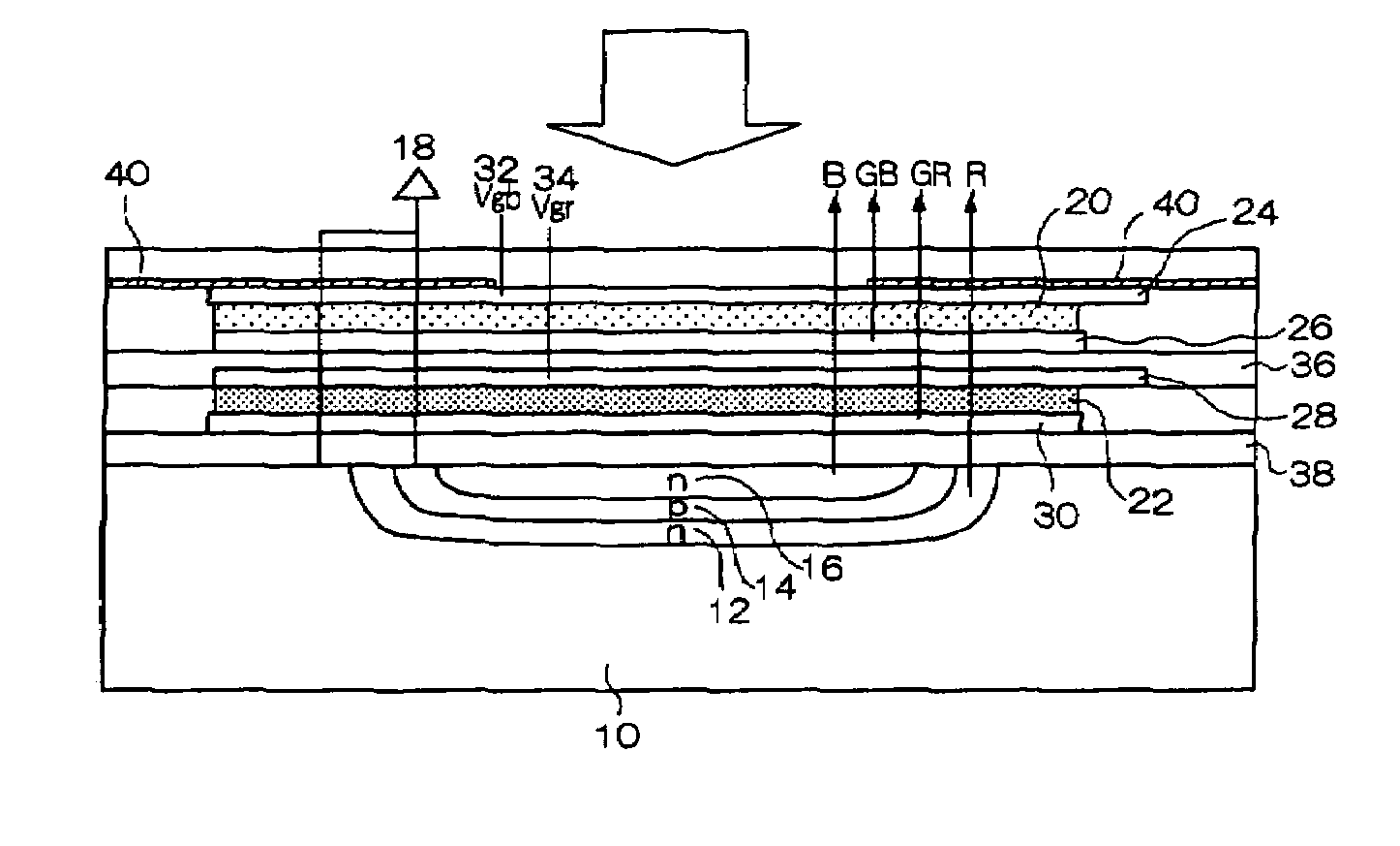
[0090]A npnp junction diode, as shown in FIG. 2, is formed and, as light receiving devices, on an outside part of the light entering side of a silicon substrate a first photoelectric conversion part and a second photoelectric conversion part are formed. The spectral sensitivity is then evaluated.

[0091]On the silicon substrate are alternately multiple stacked, from the light entering side, a p-type region of first photoelectric conversion part, and an n-type region of a second photoelectric conversion part, being of an opposite conductivity type to the first photoelectric conversion part. The respective depths of the pn junctions of the silicon substrate are made 0.151 μm, 0.20 μm, 1.3 μm, and 2.4 μm. The doping densities are, in order from the light entering side, made 1×1018 cm31 (p), 5×1017 cm−3 (n), 1×1017 cm−3 (p), 1×1016 cm−3 (n), and 1×1015 cm−3 (p-type substrate).

First Photoelectric Conversion Part

[0092]The depletion layers formed of p-n ju...

example 2

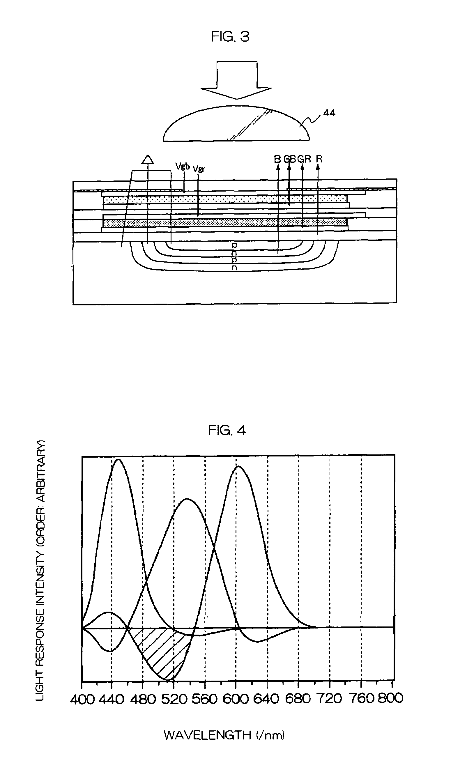
[0098]The light receiving device of Example 1 is used, and the second signal calculation is carried out as shown below.

Second Signal Calculation

Ib″=Ib−0.03 Ig−0.23 Ir

Ig″=−0.08 Ib+0.35 Ig−0.08 Ir+0.4 Igb

Ir″=−0.015 Ib+Ir−0.25 Igb

[0099]Here Ib″, Ig″ and Ir″ are respectively the strengths of the blue, green and red signals calculated for Example 1 which have been additionally corrected. Normally, when such a matrix method of calculation is carried out for signals, noise is not calculated sufficiently and S / N ratio is reduced. However, since in the invention the RGB color separation is superior, the non-diagonal elements (coefficients of Ig and Ir which occur in Ib″, the coefficients of Ib and Ir which occur in Ig″, and the coefficients of Ib and Ig which occur in Ir″) are sufficiently small, and without a large reduction in the S / N ratio all of the negative spectral sensitivity can be realized.

[0100]The corrected blue, green and red signal strengths according to this calculation are sho...


PUM


Abstract

A light receiving device and an image pickup device in which a plurality of light receiving devices are arranged are provided. The light receiving device comprises a single semiconductor substrate and a light receiving device that has a first photoelectric conversion part and a second photoelectric conversion part. The single semiconductor substrate comprises regions of a first conductivity type and regions of a second conductivity type in an alternately multiply stacked manner. Depths of each of the junction surfaces between the regions of first conductivity type and second conductivity type are formed at depths such that light mainly in the blue or red wavelength regions can be photo-electrically converted. The respective detected wavelengths of the first photoelectric conversion part and second photoelectric conversion part are longer than the central wavelength of the blue wavelength region, and shorter than the central wavelength of the red wavelength region.

Description

CROSS-REFERENCE TO RELATED APPLICATION[0001]This application claims priority under 35 USC 119 from Japanese Patent Application Nos. 2004-225848, the disclosures of which are incorporated by reference herein.BACKGROUND OF THE INVENTION[0002]1. Field of the Invention[0003]The present invention relates to a color light receiving device and an image pickup device.[0004]2. Description of the Related Art[0005]As conventional light receiving devices, metal oxide semiconductor (MOS) capacitors and pn junction diodes made of semiconductors such as crystalline silicon, amorphous silicon, GaAs, or the like, are generally used. These light receiving devices can also be utilized as photoelectric conversion sections in image pickup devices, such as charge coupled devices (CCD) and complementary metal oxide semiconductors (CMOS). Although CCD and CMOS sensors are different from each other in signal reading-out method, however, for either image pickup device, a light receiving device having the sam...

Claims


Application Information

Patent Timeline
Patent Type & Authority Patents(United States)
IPC IPC(8): H01L31/0232
CPCH01L27/14621H01L27/14643H01L27/14831H01L27/14647
Inventor YOKOYAMA, DAISUKEFUKUNAGA, TOSHIAKI
Owner FUJIFILM HLDG CORP
Why Eureka
Try Eureka