

Plasma processing apparatus, electrode plate for plasma processing apparatus, and electrode plate manufacturing method
a plasma processing apparatus and electrode plate technology, applied in the field of plasma processing apparatus, can solve the problems of energy loss, high resistivity member used for the main surface central portion of an rf electrode may consume too much rf power as joule heat, etc., and achieve the effect of improving the plasma density uniformity
- Summary
- Abstract
- Description
- Claims
- Application Information
AI Technical Summary
Benefits of technology
Problems solved by technology
Method used
Image

Examples
first embodiment
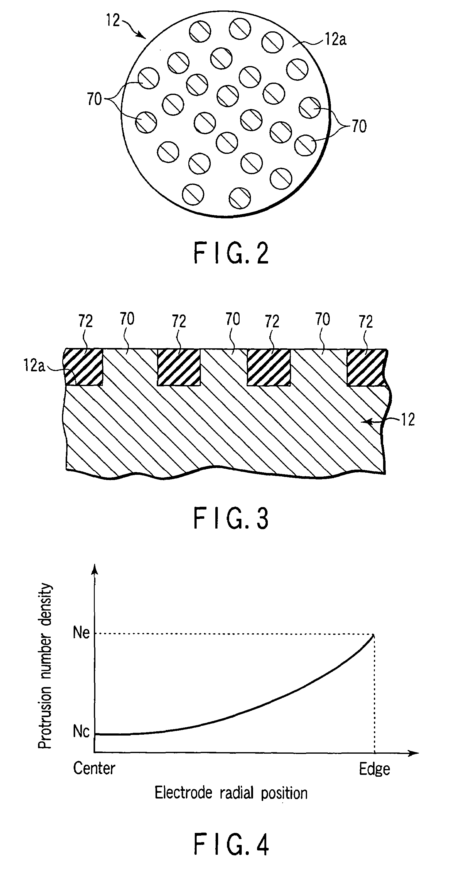
[0100]FIG. 2 is a plan view showing a susceptor structure (susceptor 12) according to the present invention. FIG. 3 is an enlarged partial and sectional side view showing the susceptor structure. FIG. 4 is a view showing a distribution characteristic concerning the protrusion number density on the susceptor structure. The main surface of the susceptor 12 (the top surface of the susceptor 12, i.e., the surface facing the plasma generation space, in this embodiment) is provided with a number of columnar protrusions 70 made of a conductor or semiconductor which have a constant size and are discretely arrayed. Each of the protrusions 70 functions as a small electrode to apply an RF power or RF electric field to plasma. Preferably, as shown in FIG. 4, the protrusions 70 are arrayed on the main surface of the susceptor 12 with a number density distribution or area density distribution such that the density gradually increases from the electrode central portion to the electrode edge portio...
second embodiment
[0128]FIG. 15 is a plan view showing an electrode structure (a susceptor 12) according to the present invention. FIG. 16 is an enlarged partial and sectional side view of the structure. FIG. 17 is a view showing a distribution characteristic concerning the recess number density on the structure. The main surface of the susceptor 12 is provided with a number of columnar recesses 80 which have a constant size and are discretely arrayed. Since the recesses 80 are dent opposite the counter electrode or plasma PZ, they are electrically coupled with the plasma PZ with a higher impedance than the top portion 12a of the main surface. Accordingly, the RF power carried by an RF current i flowing through the surface layer on the main surface of the susceptor 12 is discharged mainly from the top portion 12a toward the plasma PZ.
[0129]As shown in FIG. 16, a dielectric body 82 is preferably disposed in the recesses 80. With this arrangement, the impedance ratio Z80 / Z12a between the recesses 80 an...
third embodiment
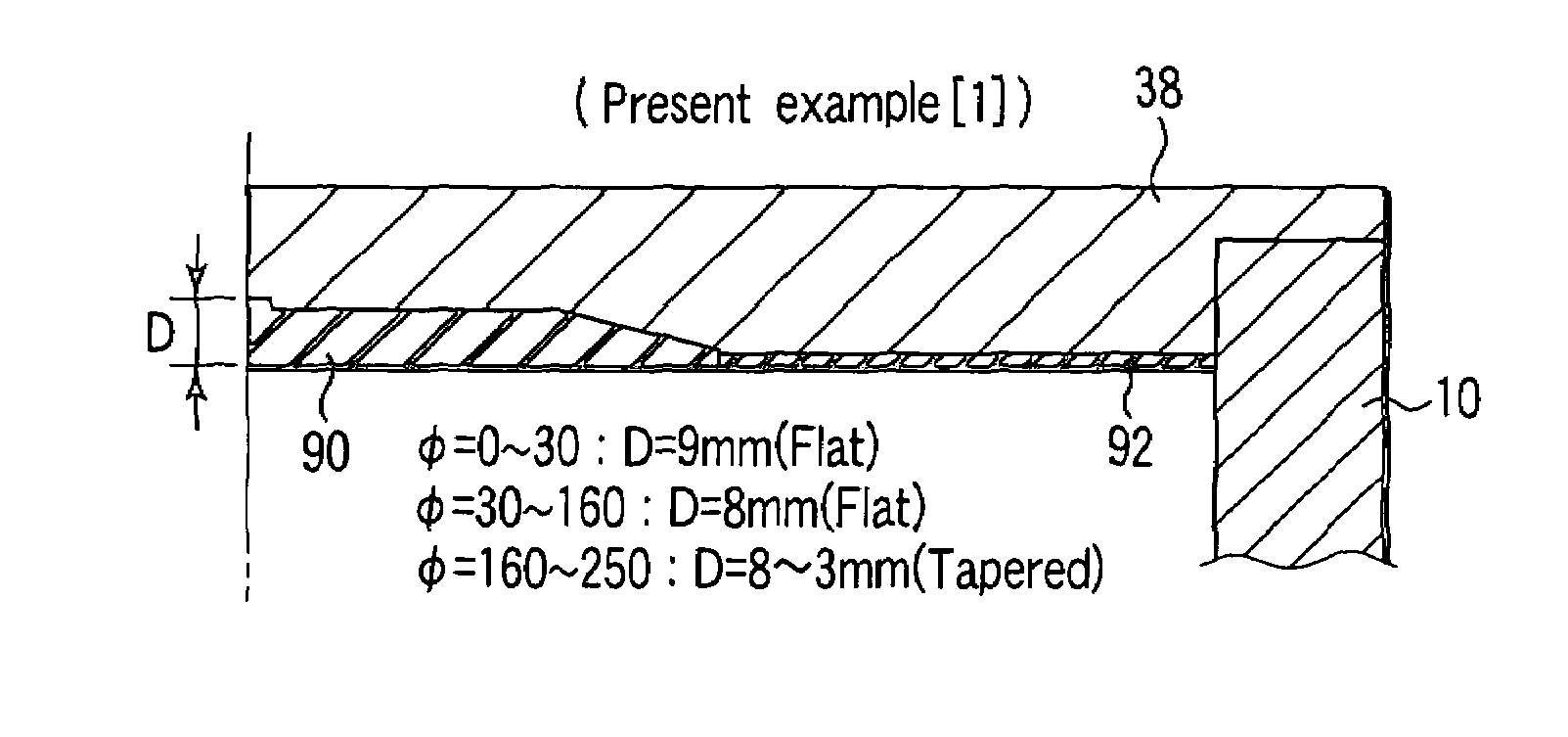
[0144]FIG. 21 is a view showing a parallel-plate electrode structure according to FIG. 22 is a view showing distribution characteristics of electric field intensity in the radial direction between electrodes, using as a parameter the film thickness at the upper electrode central portion of the parallel-plate electrode structure shown in FIG. 21. The film thickness at the electrode central portion is one of the important parameters among distribution characteristics of the film thickness of the dielectric film 90. As shown in FIG. 21, in the parallel-plate electrode structure including an upper electrode 38 with a circular dielectric film 90 disposed thereon, the distribution of electric field intensity in the radial direction between the electrodes was obtained by simulation, using as a parameter the film thickness Dc at the upper electrode central portion.
[0145]In this simulation, it was assumed that the target substrate was a semiconductor wafer with a diameter of 300 mm, the upp...
PUM
| Property | Measurement | Unit |
|---|---|---|
| frequencies | aaaaa | aaaaa |
| frequencies | aaaaa | aaaaa |
| frequency | aaaaa | aaaaa |
Abstract
Description
Claims
Application Information