Filter module and communication apparatus
a filter module and communication device technology, applied in the field of filter modules, can solve the problems of large circuit, communication failure or other malfunction, leakage of signals at frequencies corresponding to filters that are not selected, etc., and achieve the effect of improving selectivity
- Summary
- Abstract
- Description
- Claims
- Application Information
AI Technical Summary
Benefits of technology
Problems solved by technology
Method used
Image

Examples
first preferred embodiment
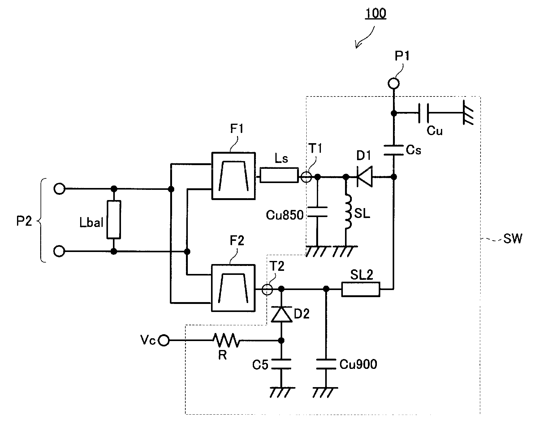
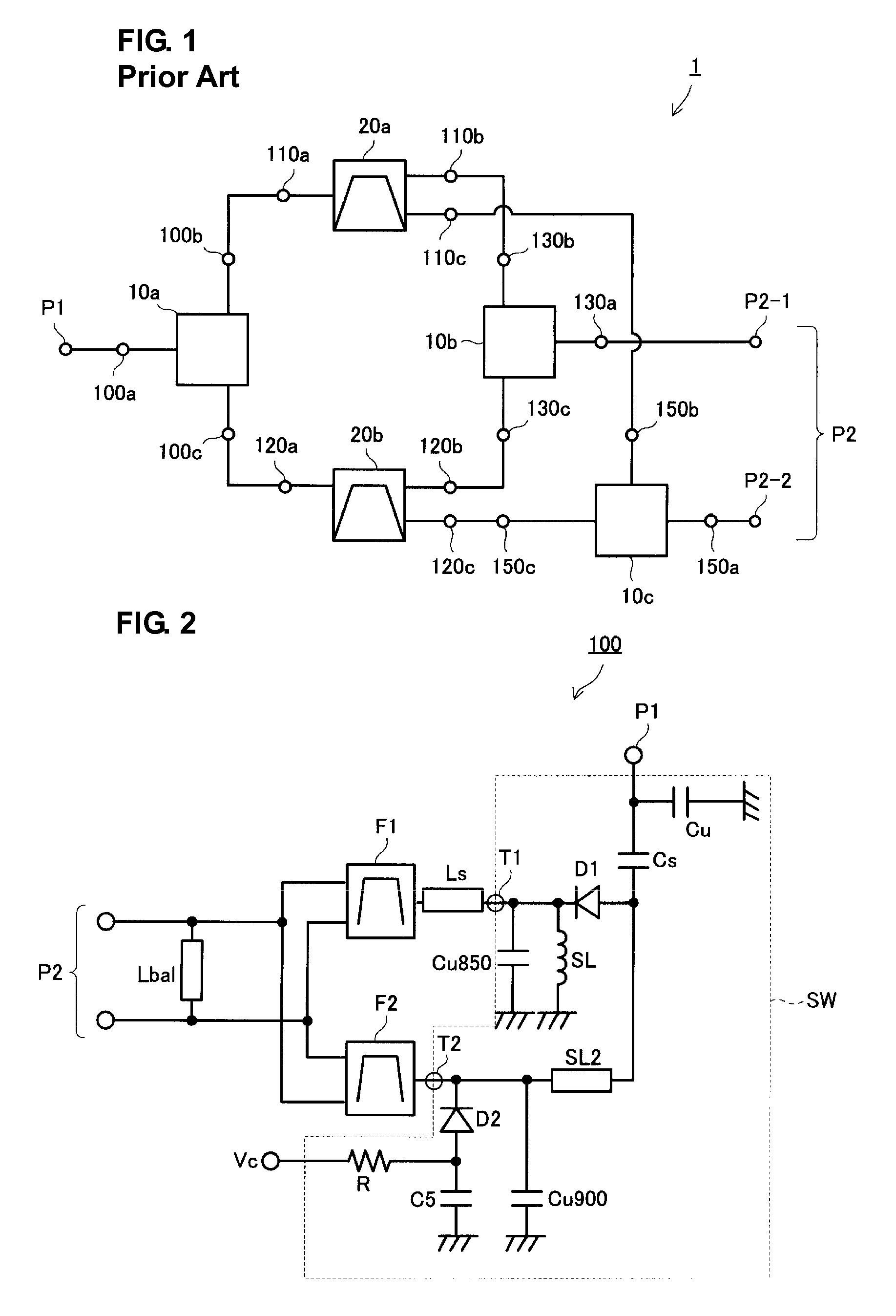
[0041]FIG. 2 is a circuit diagram illustrating a filter module according to a first preferred embodiment of the present invention. The filter module 100 includes a first input / output port P1 arranged to input and output a signal in an unbalanced state, a second input / output port P2 arranged to input and output a signal in a balanced state, and a control terminal Vc arranged to switch frequency bands. The filter module 100 primarily includes a first filter F1, a second filter F2, and a switch circuit SW.
[0042]The switch circuit SW includes a common input / output portion connected to the first port P1, a first input / output portion T1, and a second input / output portion T2. The first filter F1 passes a signal in a first frequency band (e.g., 850 MHz) and is provide between the first input / output portion T1 of the switch circuit SW and the second port P2. The second filter F2 passes a signal in a second frequency band (e.g., 900 MHz) and is provided between the second input / output portion...
second preferred embodiment
[0064]FIG. 8 is a circuit diagram of a filter module according to a second preferred embodiment of the present invention. This filter module 100 includes a first input / output port P1 arranged to input and output a signal in an unbalanced state, a second input / output port P2 arranged to input and output a signal in an unbalanced state, and a control terminal Vc arranged to switch frequency bands. The filter module 100 primarily includes a first filter F1, a second filter F2, and a switch circuit SW.
[0065]The switch circuit SW includes a common input / output portion connected to the first port P1, a first input / output portion T1, and a second input / output portion T2. The first filter F1 passes a signal in a first frequency band (e.g., 850 MHz) and is provided between the first input / output portion T1 of the switch circuit SW and the second port P2. The second filter F2 passes a signal in a second frequency band (e.g., 900 MHz) and is provided between the second input / output portion T2 ...
third preferred embodiment
[0077]FIG. 12 illustrates a configuration of a high-frequency circuit portion of a quadband mobile phone. This high-frequency circuit portion includes a triple-band chip set 103, a balanced-unbalanced filter module 100, a triple-band antenna switch module 101, and an antenna 102. The antenna switch module 101 is an antenna switch for GSM900 / DCS1800 / PCS1900, and the antenna 102 is shared for these frequency bands. The filter module 100 is connected to a GSM port, and GSM850 and GSM900 are switched using this filter module 100. The triple-band chip set 103 is a chip set for GSM900 / DCS1800 / PCS1900 and operates as an RF (high-frequency) front-end circuit for these the bands. It is also possible to configure a mobile phone by connecting a baseband chip (not shown) to the triple-band chip set 103 and providing an input / output portion in the baseband chip.
[0078]In this example, the balanced input / output port of the filter module 100 is indicated by two terminals since it performs balanced ...
PUM
 Abstract
Description
Claims
Application Information
 - R&D
- Intellectual Property
- Life Sciences
- Materials
- Tech Scout
- Unparalleled Data Quality
- Higher Quality Content
- 60% Fewer Hallucinations
Browse by: Latest US Patents, China's latest patents, Technical Efficacy Thesaurus, Application Domain, Technology Topic, Popular Technical Reports.
© 2025 PatSnap. All rights reserved.Legal|Privacy policy|Modern Slavery Act Transparency Statement|Sitemap|About US| Contact US: help@patsnap.com