Top-emitting device and illumination device

a top-emitting device and illumination device technology, applied in the direction of discharge tube/lamp details, discharge tube luminescnet screens, organic semiconductor devices, etc., can solve the problems of oleds, structural elements, and oleds that are not limited in their performance capacity, and luminous efficiency is restricted in principle by loss mechanisms, so as to improve light extraction and production economic

Active Publication Date: 2009-09-15
NOVALED GMBH
View PDF10 Cites 7 Cited by
  • Summary
  • Abstract
  • Description
  • Claims
  • Application Information

AI Technical Summary

Benefits of technology

[0020]It is the task of the invention to provide a top-emitting device with an improved light extraction which can be produced economically and which is suitable for a mass production process.

Problems solved by technology

It is generally known that conventional OLEDs only emit about 25% of the generated light, while the major part remains in optical modes of the substrate or the organic layers, and is subsequently lost in the process.
Structural elements on the basis of OLEDs, however, which are deposited on a reflecting base contact, so-called top-emitting OLEDs, are not limited in their performance capacity by losses in the transparent substrate.
Nevertheless, in this case also, the luminous efficiency is restricted in principle by the loss mechanisms because a major part of the emitted light “is captured” now within the organic layers of the OLED due to total reflection.
However, this also means that only particularly inexpensive methods can be selectable in any event for the increase of light extraction.
With the construction of OLEDs of this size, however, there is a problem with the electrode conductivity of the transparent electrode of the device.
For large-surface OLEDs, however, significantly smaller layer resistances are required because relatively high currents have to be transported through the electrodes and, thus, a significant voltage drop can occur across the electrodes, insofar as these have very small resistances smaller than 1 Ω / ∀, for example.
Due to the layer resistance of the ITO, with OLED surfaces of even a few square centimeters, this effect leads to significant luminance decays.
With the use of transparent ITO-coated substrates with a metal reinforcement, however, a passivation of the metal tracks with an insulating layer is necessary because short-circuits can otherwise occur between the bottom and the top electrode of the device.
Corresponding conductivities can, however, only be achieved with layer thicknesses which then only have a very low level transparency or are not transparent at all.
The conductivity of the transparent electrode is thus also inadequate here in order to transport the current flowing in the OLED without significant voltage losses, insofar as the device exceeds a certain size as would seem necessary for illumination applications.
However, such a solution presupposes a more complex structure of the substrate as well as additional masking steps.
For this reason, it can be assumed that top-emitting structures are of major interest in the field of illumination applications, among other things also because of the option of dispensing with ITO as a material, which is a significant cost factor for OLEDs.
Up to the present, it was not possible to commercialize the OLED technology for applications as illuminating elements, particularly in view of the fact that efficiencies and price of OLEDs are not yet competitive.
However, these methods are based on relatively complex process steps, photolithography for example.
For top-emitting OLED structures, however, structured bottom electrodes are deployed according to the state of the art by means of complex methods (refer to GB 2390215 A), for example photolithography, and these bottom electrodes are not selectable for economical mass production.
In particular the roughness of the bottom electrode is a problem for a processing of OLEDs because very thin overall layer thicknesses of approximately 100 nm are normally used for the zone of the organic layers in the OLED stack, through which there is a danger of short-circuiting between the electrodes.

Method used


Image

  • Top-emitting device and illumination device
  • Top-emitting device and illumination device
  • Top-emitting device and illumination device

Examples


Embodiment Construction

[0035]The invention is explained as follows in greater detail on the basis of embodiment examples with reference to the Figures of a drawing. The Figures show the following:

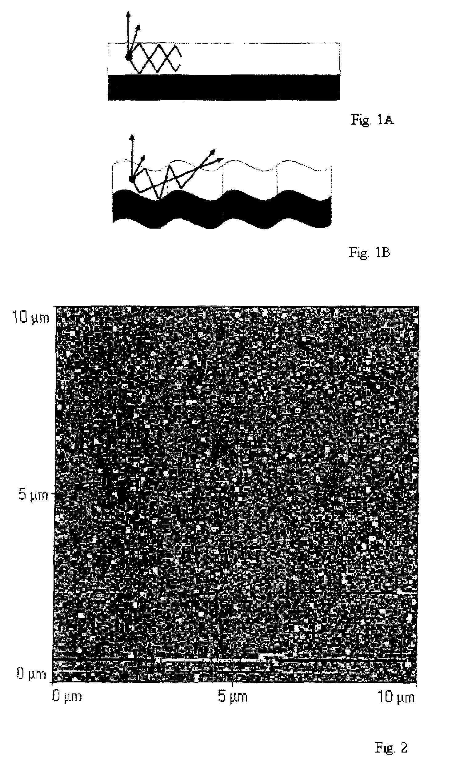
[0036]FIG. 1A Schematic illustration to explain a light reflection on a plane surface;

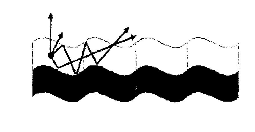
[0037]FIG. 1B Schematic illustration to explain a light reflection on a surface provided with a surface structure;

[0038]FIG. 2 Experimental results for a measurement of a surface structure by means of scanning force microscopy;

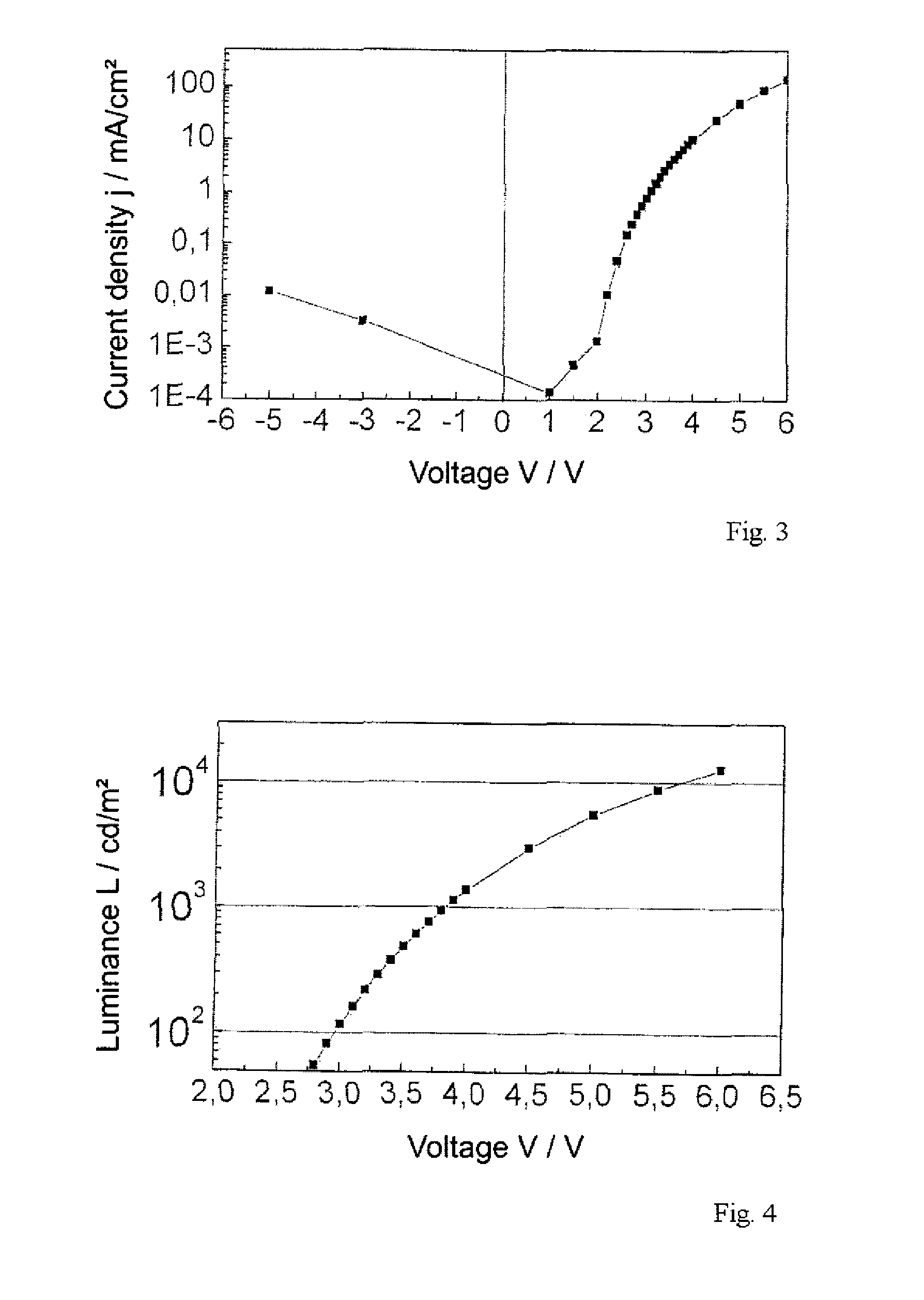
[0039]FIG. 3 A current density—voltage—characteristic for a top-emitting device;

[0040]FIG. 4 A luminance—voltage—characteristic for the top-emitting device;

[0041]FIG. 5 A graphic illustration of the luminance as a factor of the operating time for the top-emitting device;

[0042]FIG. 6 A schematic illustration for a surface configuration of an embossing stamp or an embossing roll; and

[0043]FIG. 7 A schematic illustration for a further surface configuration of an embossing stamp or an embossing roll.

[0044]FIG....


PUM


Abstract

The invention refers to a top-emitting device, particularly organic light-emitting diode having a layer arrangement applied on a substrate, which layer arrangement comprises a bottom electrode arranged on the substrate and a top electrode through which a light emission is effected, and also a stack of organic layers arranged between the bottom electrode and the top electrode where, at the bottom electrode, a surface facing towards the stack of organic layers is formed in light-reflecting fashion at least in a partial region and being provided with a surface structure that defines a reflection of light generated in the stack of organic layers at the bottom electrode, and where the surface structure is formed by means of mechanical shaping.

Description

CROSS-REFERENCE TO RELATED APPLICATION[0001]Applicants hereby claim priority under 35 U.S.C. 119(a) to European Patent Application No. 05017542.1, filed Aug, 11, 2005, the disclosure of which is expressly incorporated herein by reference in its entirety.[0002]The invention refers to a top-emitting device, in particular an organic light-emitting diode, having a layer arrangement applied on a substrate, which layer arrangement comprises a bottom electrode arranged on the substrate and a top electrode through which a light emission is effected, and also a stack of organic layers arranged between the bottom electrode and the top electrode, as well as an illumination device.BACKGROUND OF THE INVENTION[0003]Organic light-emitting diodes, which when abbreviated are also and usually designated as OLEDs, have in particular in an embodiment for white light generation a high potential for applications in the field of illumination and displays. Substantial improvements have been achieved in thi...

Claims


Application Information

Patent Timeline
Patent Type & Authority Patents(United States)
IPC IPC(8): H01J1/62
CPCH01L51/5203H01L51/5268H01L2251/5315H10K50/805H10K50/854H10K2102/3026
Inventor MURANO, SVENBIRNSTOCK, JAN
Owner NOVALED GMBH
Why Eureka
Try Eureka