Voltage controlled oscillator and wireless transceiver using the same
a voltage control and wireless transceiver technology, applied in the direction of oscillation generators, angle modulation details, resonance circuit tuning, etc., can solve the problems of inability to deal with the above various communication frequencies, increase in current consumption or chip area, and inability to realize the above object by a single voltage control oscillator, etc., to achieve the effect of reducing power consumption, reducing power consumption for long-time operations, and reducing the siz
- Summary
- Abstract
- Description
- Claims
- Application Information
AI Technical Summary
Benefits of technology
Problems solved by technology
Method used
Image
Examples
first embodiment
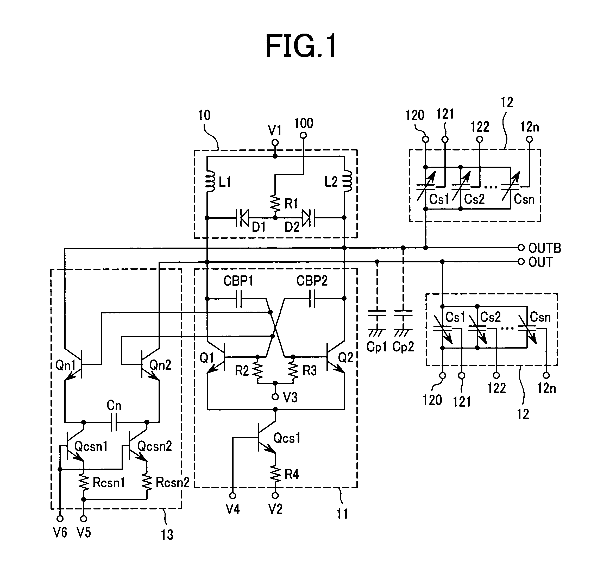
[0039]FIG. 1 shows a first embodiment according to the present invention. A voltage controlled oscillator includes a differential LC resonant circuit 10, a differential negative conductance generator circuit 11, two capacitor banks 12, parasitic capacitors Cp1 and Cp2, and a differential negative impedance circuit 13. The respective positive phase terminals+ and the respective negative phase terminals−of the differential LC resonant circuit 10, the differential negative conductance generator circuit 11, and the differential negative impedance circuit 13 are connected to each other, respectively, to thereby form a positive phase resonation node OUT (first terminal) and a negative phase resonation node OUTB (second terminal). Those two capacitor banks 12 are connected to the resonation nodes OUT and OUTB, respectively, and those capacitor banks 12 are integrated into a differential capacitor bank. The parasitic capacitors Cp1 and Cp2 are disposed on the wires of the resonation nodes O...
second embodiment
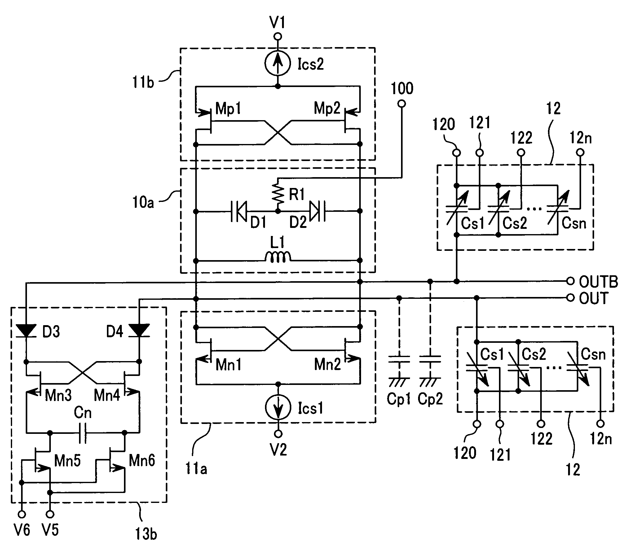
[0059]FIG. 5 shows the present invention. The first embodiment shown in FIG. 1 is structured as the bipolar voltage controlled oscillator whereas this embodiment is structured as an MOS voltage controlled oscillator using the MOS transistor. This embodiment will be described below. The same structures as those of the first embodiment will be omitted from description. In the present specification, in the bipolar transistor and the MOS transistor, the bases and the gates are described as the input terminals, the collectors and the drains are described as the output terminals, and the emitters and the sources are described as the ground terminals.
[0060]Referring to FIG. 5, the negative conductance generator circuit includes two circuits of a negative conductance generator circuit 11a (first negative conductance generator circuit) and a negative conductance circuit 11b (second negative conductance generator circuit) which are used complementarily. The negative conductance generator circ...
PUM
 Abstract
Description
Claims
Application Information


