Unlock instant, AI-driven research and patent intelligence for your innovation.
Method of fabricating capacitor over bit line and bottom electrode thereof
Active Publication Date: 2009-09-22
PROMOS TECH INC
View PDF2 Cites 2 Cited by
Summary
Abstract
Description
Claims
Application Information
AI Technical Summary
This helps you quickly interpret patents by identifying the three key elements:
Problems solved by technology
Method used
Benefits of technology
Benefits of technology
This method simplifies the capacitor fabrication process, ensuring reliable electrical connections and maintaining the required dielectric properties, thereby enhancing the compatibility and efficiency of the semiconductor process.
Problems solved by technology
However, according to the foregoing description of the method of fabricating the capacitor-terminal contacts, several complicated processing steps for forming the capacitor.
Method used
Image
Click on the blue label to locate the original text in one second.
Reading with bidirectional positioning of images and text.
Examples
first embodiment
[0061]FIGS. 6-1 through 10-2 are diagrams showing the steps for fabricating the lower electrode of a capacitor according to the present invention.
[0062]First, as shown in FIGS. 6-1, 6-2 and 6-3, FIG. 6-2 is a schematic cross-sectional view along the line II-II of FIG. 6-1. FIG. 6-3 is a schematic cross-sectional view along the line III-III′ of FIG. 6-1.
[0063]In FIGS. 6-1, 6-2 and 6-3, the locations of the substrate 100, the active region 102, the isolation region 104, the word line 106, the landing plug contact 108, the first dielectric layer 110 and the second dielectric layer 112 are identical to the ones in FIGS. 1-1, 1-2 and 1-2 and are labeled similarly. The first dielectric layer 110 is formed in portions between the word lines 106 and the landing plug contact 108 is formed in another portion between the word lines. The steps for forming the structure shown in FIGS. 6-1, 6-2 and 6-3 include, for example, depositing a first dielectric layer 110 on the surface of the substrate 1...
second embodiment
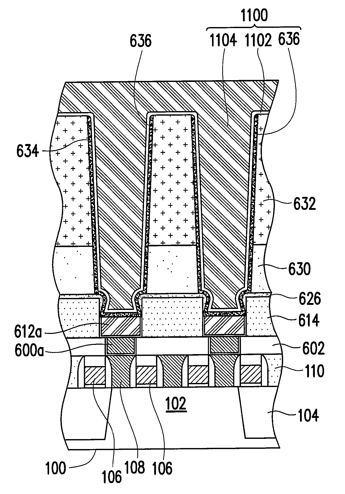
[0070]FIG. 11 is a schematic cross-sectional view of a capacitor over bit line (COB) according to the present invention.
[0071]As shown in FIG. 11, the method of fabricating the capacitor over bit line (COB) 1100 may refer to the first embodiment up to the formation of the lower electrode (that is, the conductive layer 636). Next, a capacitor dielectric layer 1102 is formed on the surface of the lower electrode. The material of the capacitor dielectric layer 1102 includes, for example, SiO2, Si3N4, Ta2O5, HfO2, HFON, ZrO2, CeO2, TiO2, Y2O3, Al2O3, La2O5, SrTiO3, BST (BaxSr1-xTiO3, wherein 0≦x≦1) or PZT (PbZrxTi1-xO3), where 0≦x≦1). Next, a top electrode 1104 is formed on the surface of the capacitor dielectric layer 1102 inside the capacitor openings 634. The material constituting the capacitor dielectric layer 1102 is selected from a group including polysilicon, AlCu, a metal and its nitride such as Ti, TiN, Ta, TaN and Al.
[0072]In summary, the fabrication of the capacitor over bit ...
PUM
Abstract
A method of fabricating a capacitor over bit line (COB) is provided. First, a substrate is provided and a plurality of word lines is formed on the substrate. Next, a plurality of landing plug contacts (LPCs) are formed between the word lines and a plurality of first contacts is then formed on the LPCs. Thereafter, a plurality of second contacts is formed on a first portions of the first contacts and a plurality of bit lines connecting a second portions of the first contacts is formed, simultaneously. An inter-layer dielectric (ILD) layer is formed on the substrate to cover the second contacts and the bit lines. Subsequently, a plurality of capacitors is formed in the ILD layer. Thus, the fabrication of the capacitor is simplified.
Description
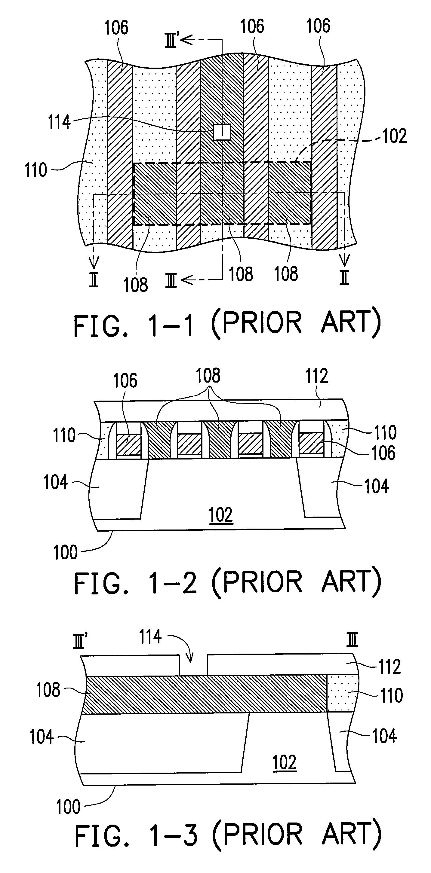
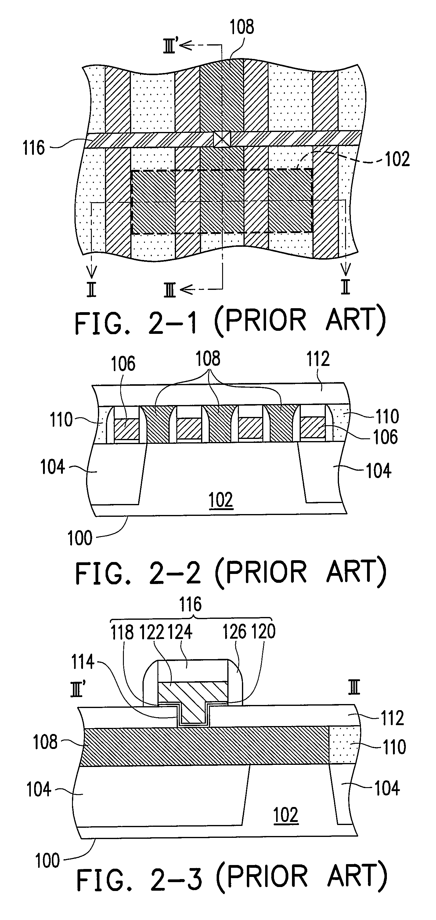
CROSS-REFERENCE TO RELATED APPLICATION[0001]This application claims the priority benefit of Taiwan application serial no. 95143931, filed on Nov. 28, 2006. All disclosure of the Taiwan application is incorporated herein by reference.BACKGROUND OF THE INVENTION[0002]1. Field of the Invention[0003]The present invention relates to a process of fabricating a capacitor, and more particularly to a method of fabricating a capacitor over bit line and a bottom electrode thereof.[0004]2. Description of Related Art[0005]Semiconductor memory devices, for example, dynamic random access memory (DRAM), normally require a capacitor so that a binary data can be stored in a memory cell according to the bias voltage provided by the capacitor. The electric charges stored in the capacitor are the basic characteristic of the DRAM. The quantity of electric charges stored in the capacitor depends on its capacitance, and the capacitance of a capacitor depends on the area of the storage electrodes, the relia...
Claims
Application Information
Patent Timeline
Application Date:The date an application was filed.
Publication Date:The date a patent or application was officially published.
First Publication Date:The earliest publication date of a patent with the same application number.
Issue Date:Publication date of the patent grant document.
PCT Entry Date:The Entry date of PCT National Phase.
Estimated Expiry Date:The statutory expiry date of a patent right according to the Patent Law, and it is the longest term of protection that the patent right can achieve without the termination of the patent right due to other reasons(Term extension factor has been taken into account ).
Invalid Date:Actual expiry date is based on effective date or publication date of legal transaction data of invalid patent.
