

Circuit and method for a gate control circuit with reduced voltage stress
- Summary
- Abstract
- Description
- Claims
- Application Information
AI Technical Summary
Benefits of technology
Problems solved by technology
Method used
Image

Examples
Embodiment Construction
[0048]The making and using of the presently preferred embodiments are discussed in detail below. It should be appreciated, however, that the present invention provides many applicable inventive concepts that can be embodied in a wide variety of specific contexts. The specific embodiments discussed are merely illustrative of specific ways to make and use the invention, and do not limit the scope of the invention.
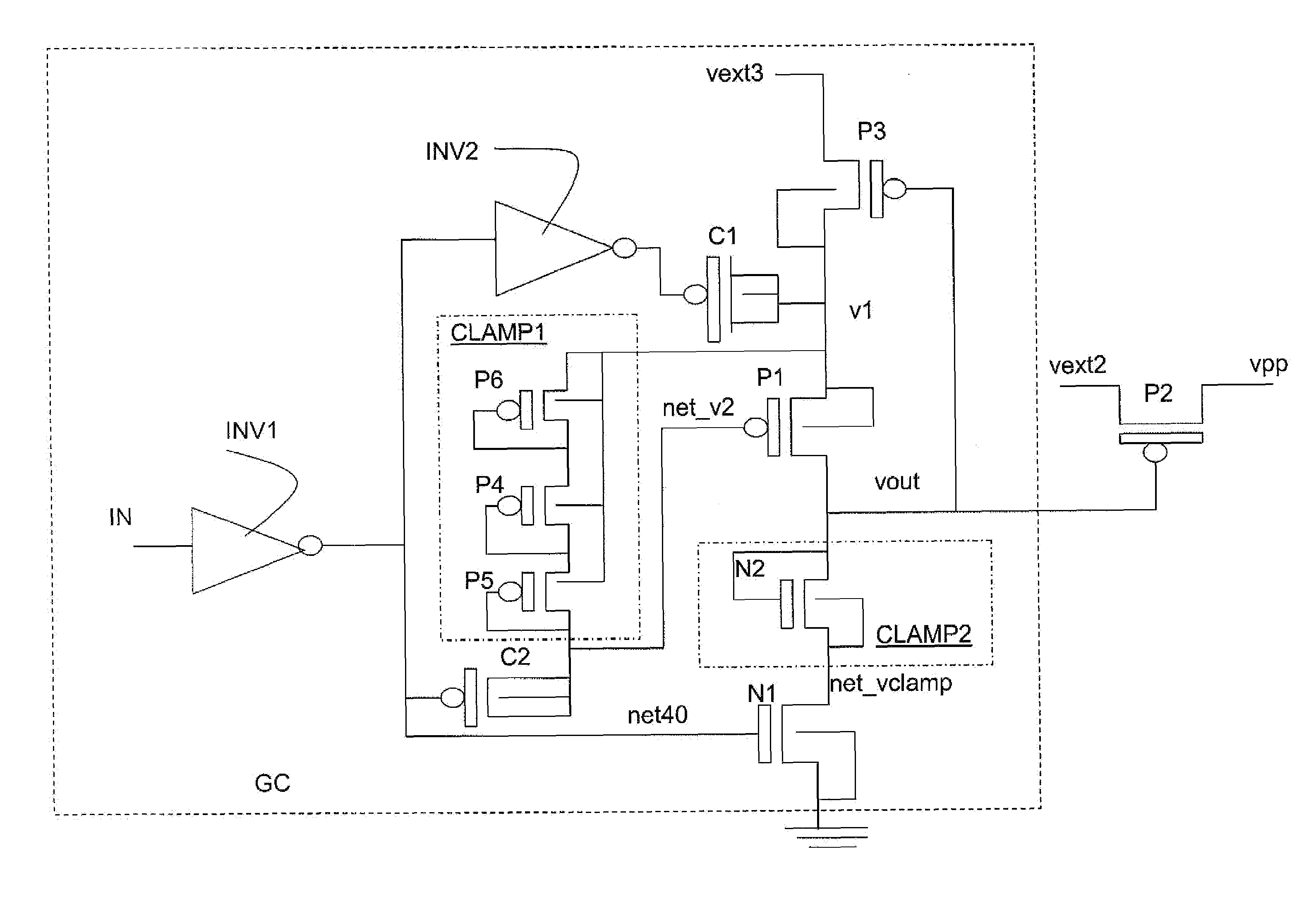
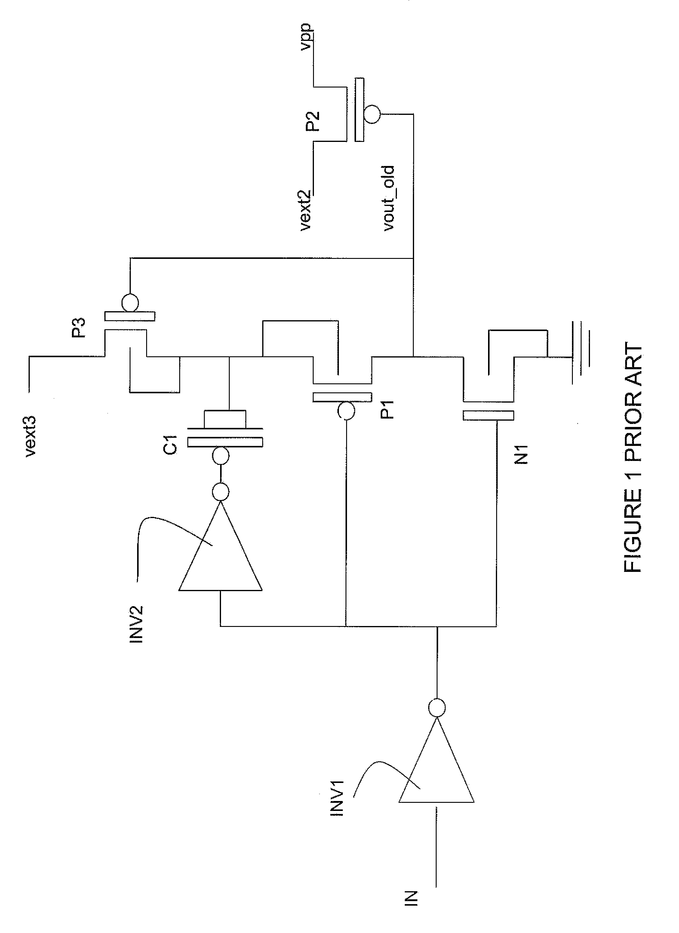
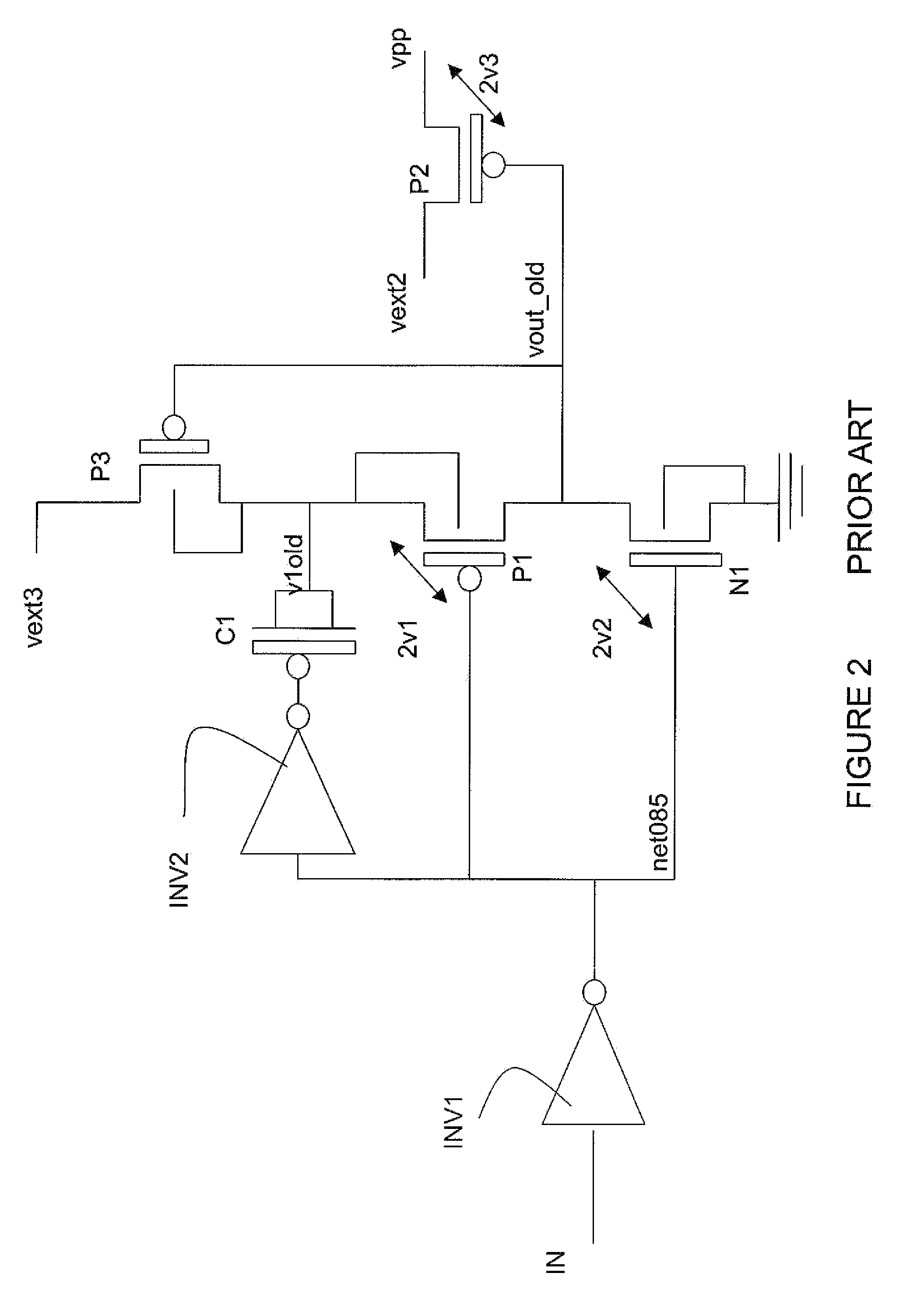
[0049]FIG. 1 depicts a prior art gate control circuit. In FIG. 1, the gate control circuit is formed by coupling a capacitor C1 (here, a MOS transistor coupled to use the gate conductor as one plate of a two-terminal capacitor and the source / drain are commonly coupled so that the channel region forms the other capacitor plate; thus the gate oxide of the transistor forms the capacitor dielectric; other alternatives are to use trench, substrate or other capacitors used in integrated circuits as is known in the art) to a time varying signal coupled from the voltage input IN thro...
PUM
 Abstract
Description
Claims
Application Information