Electro-optical device and electronic equipment having touch panel with resin having particular elastic modulus

a technology of electronic equipment and touch panel, applied in the direction of electric digital data processing, instruments, computing, etc., can solve the problems of input malfunction, weak shock resistance of touch panel device configured from one sheet of glass, and possible attenuation of surface acoustic waves, so as to prevent the shattering of the touch panel, high reliability, and high performance

Active Publication Date: 2009-09-22
138 EAST LCD ADVANCEMENTS LTD
View PDF11 Cites 153 Cited by
  • Summary
  • Abstract
  • Description
  • Claims
  • Application Information

AI Technical Summary

Benefits of technology

[0016]An advantage of some aspects of the invention is to provide an electro-optical device and electronic equipment which accurately detect the position at which the user imparts pressure, and which prevent input malfunctions.

Problems solved by technology

There is the problem that a touch panel device configured from one sheet of glass is weak in shock resistance, and particularly that it can be split by minor shocks if thinner glass is contrived.
When the transparent resin film does not adequately bend in response to user pressure, it is not possible to cause attenuation of the surface acoustic waves that are propagated on the surface of the glass substrate.
In such a case, there is the problem that the position pressed by the user cannot be accurately detected, and input malfunctions occur.
This becomes noise that causes the touch panel to malfunction.

Method used


Image

  • Electro-optical device and electronic equipment having touch panel with resin having particular elastic modulus
  • Electro-optical device and electronic equipment having touch panel with resin having particular elastic modulus
  • Electro-optical device and electronic equipment having touch panel with resin having particular elastic modulus

Examples


first embodiment

Liquid Crystal Display Device

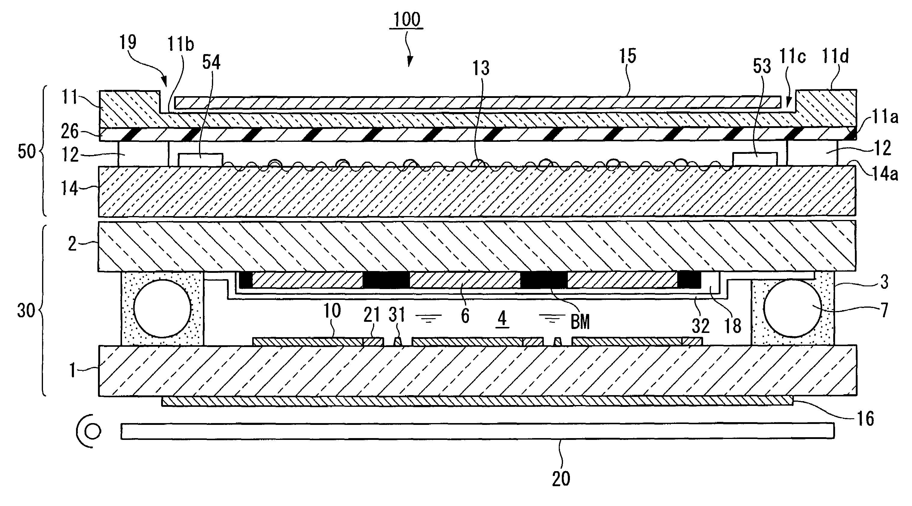
[0053]First, an explanation is given regarding the configuration of a liquid crystal display device having the touch panel pertaining to the first embodiment of the present invention. FIG. 1 is a sectional view that schematically shows the schematic configuration of a liquid crystal display device 100 having the touch panel pertaining to the first embodiment. In each of the drawings used in the following descriptions, the scale of the various members has been suitably modified to give each member a size that is readily perceivable.

[0054]Roughly speaking, the liquid crystal display device 100 (electro-optical device) of FIG. 1 is composed of a liquid crystal display panel 30 (electro-optical panel) and a touch panel 50.

[0055]First, an explanation is given regarding the configuration of the liquid crystal display panel. Additionally, the faces of an element substrate 1 and color filter substrate 2 on a liquid crystal layer 4 side is referred to as inner fa...

second embodiment

[0094]Next, a second embodiment is described with reference to drawings.

[0095]In the foregoing first embodiment, the touch panel is configured from the pairing of a first touch panel substrate and a second touch panel substrate. In contrast, the present embodiment differs in that the touch panel is configured from a single thin-plate substrate. As the remaining basic configuration of the liquid crystal display device is identical to that of the aforementioned first embodiment, the same code numbers are given to shared components, and detailed description thereof is omitted.

[0096]FIG. 6 is a sectional view showing the schematic configuration of the liquid crystal display device 100 pertaining to the present embodiment.

[0097]As shown in FIG. 6, a thin-plate substrate 11 (touch panel substrate) is arranged on the outer face 2a side of the color filter substrate 2 of the liquid crystal display panel 30 (the face of the color filter substrate 2 which is opposite the liquid crystal layer ...

third embodiment

[0101]Next, the present embodiment is described with reference to drawings.

[0102]In the foregoing first embodiment, the input part pressed by the finger of the user was configured from a touch panel substrate composed of glass. In contrast, the present embodiment differs in that the input part pressed by the finger of the user is configured from resin film and a polarization plate. As the remaining basic configuration of the liquid crystal display device is identical to that of the aforementioned first embodiment, the same code numbers are given to shared components, and detailed description thereof is omitted.

[0103]FIG. 7 is a sectional view showing the schematic configuration of a liquid crystal display device 100 pertaining to the present embodiment.

[0104]As shown in FIG. 7, the touch panel substrate 14 is arranged on the outer face 2a side of the color filter substrate 2 of the liquid crystal display panel 30 (the face of the color filter substrate 2 which is opposite the liquid...


PUM

PropertyMeasurementUnit
Young's modulusaaaaaaaaaa
elastic modulusaaaaaaaaaa

Abstract

An electro-optical device includes: an electro-optical panel having a first substrate, a second substrate, and an electro-optical substance interposed between the first and the second substrates; a third substrate arranged on the second substrate; a fourth substrate having a flexibility and arranged on the third substrate via a spacer; a position detector provided on the third substrate and detecting a pressed position on the fourth substrate based on changes in surface waves generated on the third substrate; and a resin film provided on the fourth substrate and opposed to the third substrate.

Description

CROSS-REFERENCE TO RELATED APPLICATION[0001]This application claims priority to Japanese Patent Application No. 2006-017330, filed Jan. 26, 2006, the content of which are incorporated herein by reference.BACKGROUND[0002]1. Technical Field[0003]This invention relates to an electro-optical device and to electronic equipment.[0004]2. Related Art[0005]In recent years, accompanying the diffusion of compact electronic information equipment such as the personal digital assistant (PDA) and palm-top computer, liquid crystal display devices in which touch panels are mounted as input devices on a liquid crystal display panel have come into wide use.[0006]As an example of this touch panel, there is known to be an ultrasonic surface acoustic wave system provided with a glass substrate, a transmitter that generates surface acoustic waves on the surface of the glass substrate, and a receiver that detects the generated surface acoustic waves.[0007]The surface acoustic waves that are propagated on t...

Claims


Application Information

Patent Timeline
Patent Type & Authority Patents(United States)
IPC IPC(8): G02F1/1335G02F1/1333G06F3/041G06F3/043
CPCG06F3/0436G02F1/13338G06F3/0354G06F3/0412G06F3/0414G06F3/0416
Inventor TAGUCHI, SATOSHISAKURAI, SHINJIFUNASAKA, TSUKASA
Owner 138 EAST LCD ADVANCEMENTS LTD
Why Eureka
Try Eureka