Packaging board and manufacturing method therefor, semiconductor module and mobile apparatus

a packaging board and manufacturing method technology, applied in the field of packaging boards, can solve the problems of difficult ion migration between wiring patterns, and achieve the effect of improving the reliability of packaging boards

Active Publication Date: 2009-09-29
III HLDG 12 LLC
View PDF11 Cites 35 Cited by
  • Summary
  • Abstract
  • Description
  • Claims
  • Application Information

AI Technical Summary

Benefits of technology

[0010]The present invention has been made in view of the foregoing circumstances, and a general purpose thereof is to provide a technology for improving the reliability of a packaging board by preventing moisture entering from the pad electrode portion from spreading over the surface of the wiring pattern.
[0012]According to this embodiment, the moisture infiltrating via the interface between the gold plating layer and the insulating layer and spreading over the surface of the wiring layer has a longer distance of spreading than a conventional structure without the stepped portion. As a result, the supply of moisture to the wiring layer in the wiring region is restricted, thus making ion migration between wiring patterns hard to occur. Consequently, the reliability of the packaging board can be improved.
[0013]In the above embodiment, the stepped portion is preferably formed in such manner that it is positioned lower than a top surface of the wiring region. With this structure, moisture is more likely to collect at the bottom part of the stepped portion, and thus the stepped portion acts as a barrier to the infiltrating moisture. This further restricts the spread of moisture from the boundary region to the wiring region of the wiring pattern. Consequently, the reliability of the packaging board can be further improved.
[0014]In the above embodiment, a surface of the wiring layer in contact with insulating layer in the boundary region is preferably roughened. In such a case, the surface of the wiring layer in the boundary region has fine asperities. Hence, the distance of infiltrating moisture spreading over the surface of the wiring pattern is longer, thus restricting the spread of moisture. Also, the fine unevenness provided on the surface of the wiring pattern improves the adhesion of the part to the insulating layer, which makes it harder for the infiltrating moisture to spread along the interface between the wiring layer in the boundary region and the insulating layer. As a result of these, the spread of moisture from the boundary region to the wiring region of the wiring layer is further restricted. Consequently, the reliability of the semiconductor module can be further improved.
[0015]In the above embodiment, the wiring layer and the insulating layer may be formed on a substrate; the wiring layer may have a gap between the wiring layer and the substrate along an edge at a side of the wiring layer in contact with the substrate; and the insulating layer may be so formed as to fill in the gap. By implementing this structure, the anchor effect of the insulating layer filling up the gap improves the adhesion between the wiring layer and the insulating layer, thus making it harder for infiltrating moisture to spread over the surface of the wiring layer in the wiring region. As a result, the reliability of the packaging board can be further improved.

Problems solved by technology

As a result, the supply of moisture to the wiring layer in the wiring region is restricted, thus making ion migration between wiring patterns hard to occur.

Method used


Image

  • Packaging board and manufacturing method therefor, semiconductor module and mobile apparatus
  • Packaging board and manufacturing method therefor, semiconductor module and mobile apparatus
  • Packaging board and manufacturing method therefor, semiconductor module and mobile apparatus

Examples


first embodiment

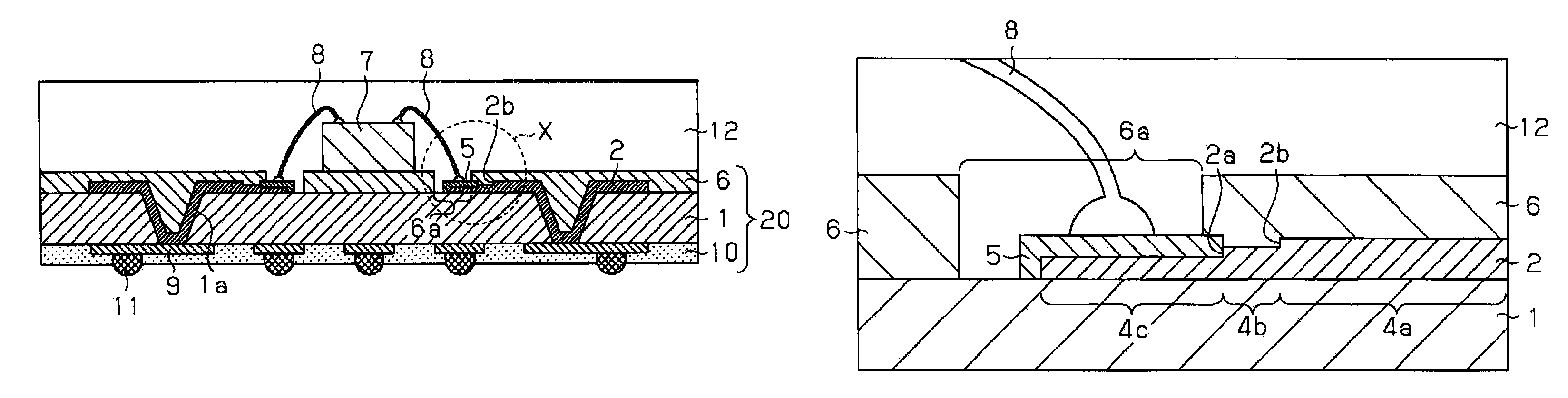
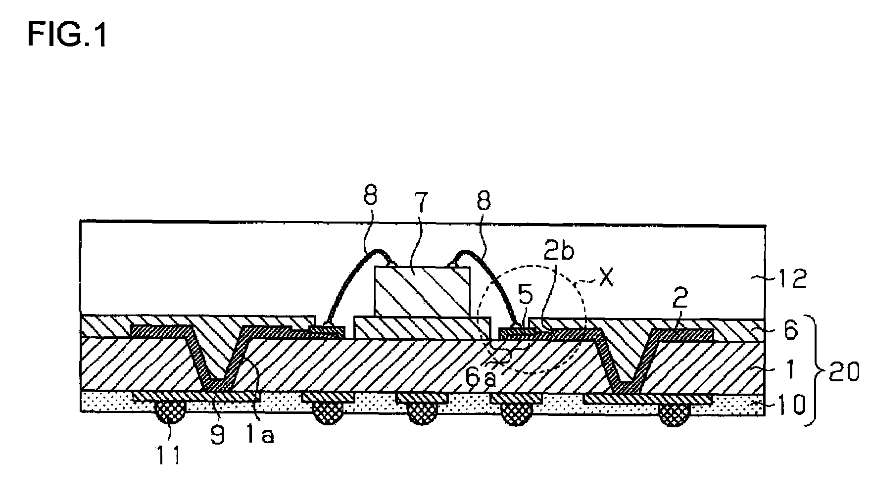
[0041]FIG. 1 is a schematic cross-sectional view showing a semiconductor module having a pad electrode according to a first embodiment of the present invention. FIG. 2 is an enlarged sectional view of a pad electrode portion (sectional area indicated by X in FIG. 1) of a semiconductor module shown in FIG. 1, and FIG. 3 is a schematic top view of a pad electrode portion of a semiconductor as shown in FIG. 1. Note that FIG. 2 is a cross section taken along the line A-A of FIG. 3.

[0042]A semiconductor module according to the first embodiment has a semiconductor device 7 mounted on the upper face of a packaging board 20 and solder balls 11, as external connection terminals, bonded to the lower face thereof. Provided on upper face of the packaging board 20 is a wiring pattern 2 of copper connected electrically to the semiconductor device 7, and provided on the lower face thereof is a wiring pattern 9 of copper to which external connection terminals are bonded. The wiring pattern 2 and th...

second embodiment

[0063]FIGS. 7A and 7B show cross sections taken along the line B-B of FIG. 3. FIG. 7A is a cross-sectional view of a semiconductor module according to the first embodiment, and FIG. 7B a cross-sectional view thereof according to a second embodiment of the present invention.

[0064]As illustrated in FIG. 7A, a wiring pattern 2 of a semiconductor module according to the first embodiment is a rectangular wiring pattern 2 formed on an insulating substrate 1 and sealed and covered by a solder resist 6. In contrast to this, a wiring pattern 2 of a semiconductor module according to the second embodiment has a skirt-shaped bottom 2c and is further provided with a gap 1b with the insulating substrate 1 along the edges of the skirt-shaped bottom 2c. Otherwise, the structure is the same as one of the first embodiment.

[0065]A semiconductor module, which has the gap 1b with the insulating substrate 1 along the edges of the skirt-shaped bottom 2c of the wiring pattern 2, can be produced by first fo...

third embodiment

[0068]FIG. 8 is a cross-sectional view of a pad electrode portion of a semiconductor module according to a third embodiment of the present invention. The difference with the first embodiment lies in that the surface of the wiring pattern 2 in the boundary region 4b and the wiring region 4a is roughened. Otherwise, the structure is the same as that of the first embodiment.

[0069]A semiconductor like this can be easily produced by roughening the surface of the wiring pattern 2 of copper by a wet process or the like after the process shown in FIG. 6B. For example, a surface treatment using an acidic chemical can create a roughened surface with fine unevenness (fine asperities). Thus the surface of the wiring pattern 2 may be roughened with fine asperities. The arithmetic mean roughness Ra of the wiring pattern after the roughening is about 0.38 μm. The Ra of the surface of the wiring pattern 2 can be measured with a stylus type surface texture measuring instrument. Note that the roughen...


PUM

PropertyMeasurementUnit
thicknessaaaaaaaaaa
thicknessaaaaaaaaaa
thicknessaaaaaaaaaa

Abstract

An advantage of the present invention is to suppress moisture infiltrating from a pad electrode portion from spreading over the surface of a wiring pattern and improve the reliability of a packaging board. The wiring pattern of the packaging board is formed on an insulating substrate and includes a wiring region, an electrode region (pad electrode) connected with a semiconductor device, and a boundary region provided between the wiring region and the electrode region. A gold plating layer is provided on the surface of the electrode region of the wiring pattern. The top surface of the boundary region of the wiring pattern is so formed as to be dented from the top surface of the wiring region of the wiring pattern, and there is provided a stepped portion in the boundary region. A solder resist is formed in such a manner as to cover part of the gold plating layer and the wiring pattern corresponding to the boundary region and the wiring region, and the solder resist has a predetermined opening through which to connect to the semiconductor device. A conductive member is connected to the gold plating layer in the electrode region, and a molded resin layer seals the entire semiconductor module.

Description

CROSS-REFERENCE TO RELATED APPLICATIONS[0001]This application is based upon and claims the benefit of priority from the prior Japanese Patent Applications No. 2006-302443, filed on Nov. 8, 2006, Japanese Patent Application No. 2007-275739, filed on Oct. 23, 2007, and Japanese Patent Application No. 2007-290839, filed on Nov. 8, 2007, the entire contents of which are incorporated herein by reference.BACKGROUND OF THE INVENTION[0002]1. Field of the Invention[0003]The present invention relates to a packaging board and, more particularly, to a packaging board having pad electrodes.[0004]2. Description of the Related Art[0005]Portable electronic devices, such as mobile phones, PDAs, DVCs, and DSCs, are today gaining an increasing variety of functions. And to be accepted by the market, they have to be smaller in size and lighter in weight, and for that reason, there is a growing demand for highly-integrated system LSIs. On the other hand, these electronic devices are expected to be easier...

Claims


Application Information

Patent Timeline
Patent Type & Authority Patents(United States)
IPC IPC(8): H01L23/12H01L23/02H01L29/40H01L23/52H01L23/04H01L23/053H01L23/48H01L23/06
CPCH01L23/295H01L24/16H01L24/48H05K1/111H05K3/243H05K3/3452H01L23/3128Y10T29/49156H01L2224/13099H01L2224/45144H01L2224/48228H01L2224/48471H01L2224/48599H01L2924/01012H01L2924/01013H01L2924/01014H01L2924/01028H01L2924/01029H01L2924/0103H01L2924/01046H01L2924/01047H01L2924/0105H01L2924/01078H01L2924/01079H01L2924/01082H01L2924/01083H01L2924/01088H01L2924/014H05K3/383H05K2201/09745H05K2203/0369H05K2203/0542Y10T29/49155H01L2924/01005H01L2924/01033H01L2224/48464H01L2224/73204H01L2224/16237H01L2224/48227H01L2924/00014H01L24/45H01L2924/00011H01L2924/181Y02P70/50H01L2224/05599H01L2924/00012H01L2224/0401
Inventor NAGAMATSU, MASAYUKIUSUI, RYOSUKE
Owner III HLDG 12 LLC
Why Eureka
Try Eureka