Semiconductor device including amplifier and frequency converter

a technology of semiconductor devices and frequency converters, which is applied in the direction of semiconductor devices, semiconductor/solid-state device details, gain control, etc., can solve the problems of noise resulting from the presence of a common impedance, the scaling up of the main body of the semiconductor device, and the inability to provide bumps which serve as external terminals on the bottom portion of the chip. , to achieve the effect of reducing the common impedance, and reducing the common im

Active Publication Date: 2009-10-27
RENESAS ELECTRONICS CORP
View PDF3 Cites 3 Cited by
  • Summary
  • Abstract
  • Description
  • Claims
  • Application Information

AI Technical Summary

Benefits of technology

[0008]It is therefore an object of the present invention to provide a semiconductor device that can be miniaturized.
[0009]Another object of the present invention is to provide a semiconductor device having improved characteristics.
[0017]Since the first common conductor portion for supplying the GND potential to the first circuit portion in the chip and the second common conductor portion for supplying the GND potential to the second circuit portion in the chip are provided over the wiring substrate, and the first and second common conductor portions are separated from each other, it becomes possible to eliminate a common impedance, while allowing each of the circuit blocks to have a common GND to be used therein. Thus, the shared use of the GND makes it possible to achieve miniaturization of the semiconductor device. By further dividing the GND correspondingly relative to the individual circuit blocks, it becomes possible to reduce the common impedance and improve the characteristics of the semiconductor device.

Problems solved by technology

In a semiconductor device having such a structure, a common lead is shared by all of the GNDs and power supply lines so that the problem of noise resulting from the presence of a common impedance occurs.
When a ring-shaped common lead is provided, bumps which serve as external terminals cannot be provided on the bottom portion of the chip, so that the problem of the scaling up of the main body of the semiconductor device also occurs.

Method used


Image

  • Semiconductor device including amplifier and frequency converter
  • Semiconductor device including amplifier and frequency converter
  • Semiconductor device including amplifier and frequency converter

Examples


embodiment 1

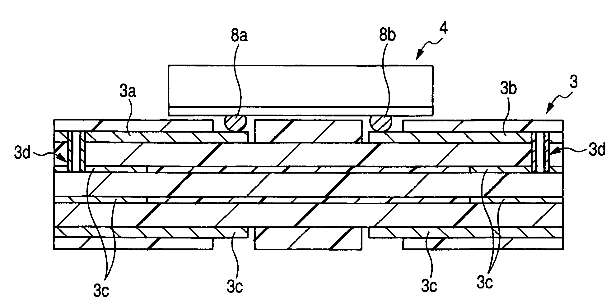
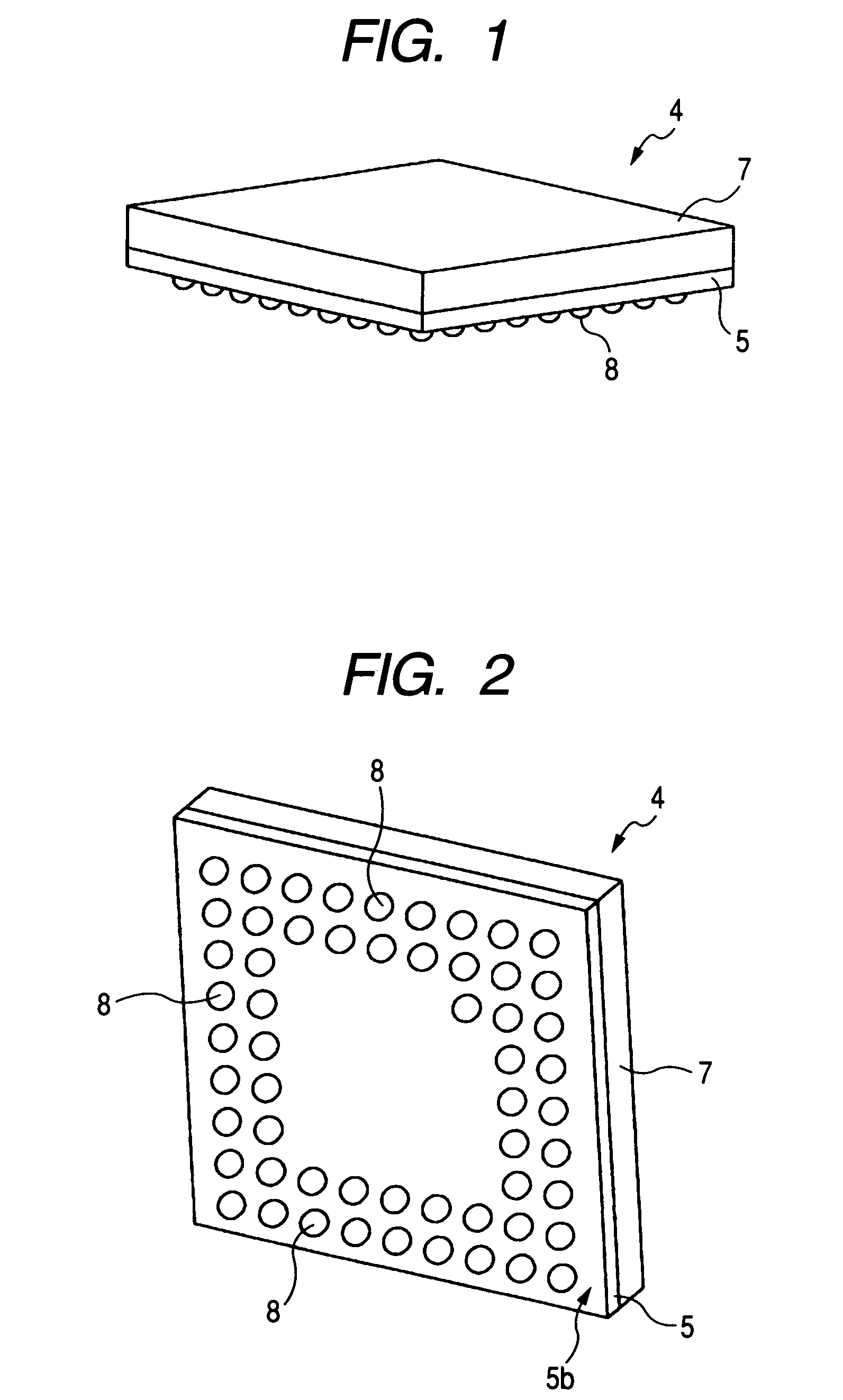
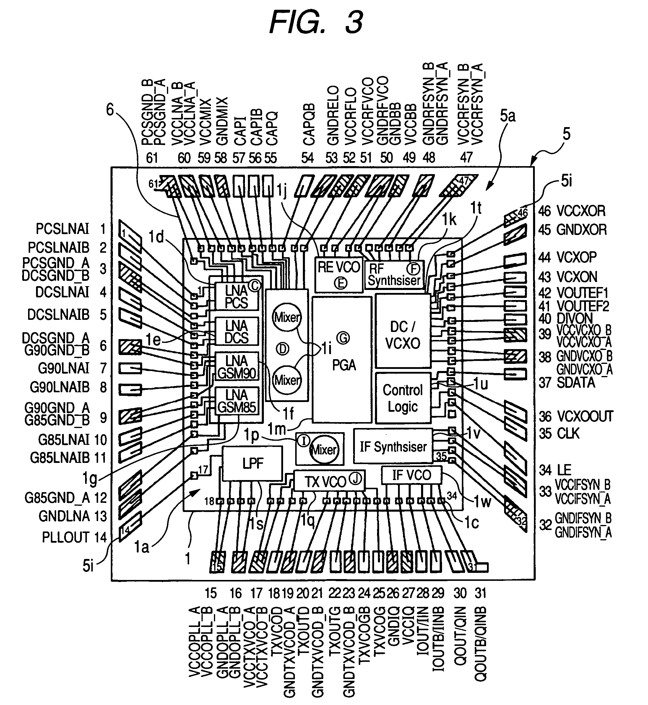
[0036]FIG. 1 is a perspective view showing an example of a structure of the semiconductor device according to a first embodiment of the present invention. FIG. 2 is a perspective view showing an example of the arrangement of terminals on the back surface of the semiconductor device shown in FIG. 1. FIG. 3 is a plan view showing an example of the structure of circuit blocks in a semiconductor chip mounted on the semiconductor device shown in FIG. 1 and an example of the connecting condition thereof with bonding electrodes. FIG. 4 is a plan view showing an example of a common GND pattern in a wiring layer on the top surface of a wiring substrate incorporated in the semiconductor device shown in FIG. 1. FIG. 5 is a bottom view showing an example of a wiring pattern in a wiring layer on the back surface of the wiring substrate shown in FIG. 4. FIG. 6 is a bottom view showing an example of the arrangement of the external terminals of the semiconductor device shown in FIG. 1. FIG. 7 is a ...

embodiment 2

[0077]FIG. 11 is a plan view showing an example of a wiring pattern in a wiring layer on the top surface of a packaging substrate incorporated in a semiconductor device according to a second embodiment of the present invention. FIG. 12 is a cross-sectional view showing a structure in which a semiconductor device, incorporating a variation using the wiring pattern shown in FIG. 11, is mounted and a plan view of a planar conductor portion. FIG. 13 is a bottom view showing the arrangement of external terminals in the semiconductor device incorporating the variation shown in FIG. 12. FIG. 14 is a circuit diagram showing an example of a no-leakage-current state in the semiconductor device incorporating the variation shown in FIG. 12.

[0078]The semiconductor device according to the second embodiment is the same semiconductor package as the RF power module 4 according to the first embodiment, in which the GND common wires are provided in separate relation corresponding to the individual cir...


PUM


Abstract

A miniaturized semiconductor device has a package substrate, a semiconductor chip mounted on the main surface of the package substrate and having plural LNAs each for amplifying a signal, an RF VCO for converting the frequency of the signal supplied from each LNA, and an IF VCO for converting the frequency of a signal supplied from a baseband. A plurality of ball electrodes are provided on the back surface of the package substrate. The package substrate is provided with a first common GND wire for supplying a GND potential to each of the LNAs, with a second common GND wire for supplying the GND potential to the RF VCO, and with a third common GND wire for supplying the GND potential to the IF VCO. The first, second, and third common GND wires are separated from each other.

Description

CROSS-REFERENCE TO RELATED APPLICATION[0001]The present application claims priority from Japanese patent application No. 2004-161300, filed on May 31, 2004, the content of which is hereby incorporated by reference into this application.BACKGROUND OF THE INVENTION[0002]The present invention relates in general to a semiconductor device; and, more particularly, it relates to a technology which is effective when applied to the miniaturization of a semiconductor device.[0003]In a conventional integrated circuit package (semiconductor device), a filter device is coupled to at least one of a power supply line for supplying power to an integrated circuit that is packaged in the package and an earth line that provides for a reduction in electromagnetic interference caused by the integrated circuit. As an example, a plurality of filter capacitors are coupled between the power supply line and the earth line within or in the vicinity of a cavity in the package (see, e.g., Patent Document 1).[00...

Claims


Application Information

Patent Timeline
Patent Type & Authority Patents(United States)
IPC IPC(8): H01L23/52H01L23/06H01L23/12H01L23/04H01L23/31H01L23/66H01L25/04H03G3/30
CPCH03G3/3036H01L23/66H01L23/3121H01L2224/45144H01L2224/16H01L2224/48227H01L2224/49171H01L2924/01079H01L2924/14H01L2924/15311H01L2924/19041H01L2924/3011H01L2924/3025H01L24/48H01L24/49H01L2924/01019H01L2224/32225H01L2224/73265H01L2924/00H01L24/45H01L2224/023H01L2224/05554H01L2924/00014H01L2224/05599H01L2924/0001
Inventor DANNO, TADATOSHINAGAMINE, TORUMORI, HIROSHIICHINOSE, TSUKASA
Owner RENESAS ELECTRONICS CORP
Why Eureka
Try Eureka