Latch circuit and semiconductor integrated circuit having the same

a technology of latch circuit and integrated circuit, which is applied in the field of latch circuit, can solve the problems of data inversion caused by noise generated by a reduction in voltage, soft error, data inversion, etc., and achieve the effect of increasing the degree of integration of the circui

Active Publication Date: 2009-11-03
PANASONIC CORP
View PDF11 Cites 22 Cited by
  • Summary
  • Abstract
  • Description
  • Claims
  • Application Information

AI Technical Summary

Benefits of technology

[0013]More preferably, the capacitor element is arranged to fill an empty space in a semiconductor integrated circuit having the latch circuit. In this manner, a degree of integration of the circuit can be increased.
[0016]Still more preferably, a semiconductor integrated circuit includes: the latch circuit; and a switching control circuit for detecting switching of operation voltages of the latch circuit to control the switching element to an ON state during a switching period. According to this, the capacitance of the storage node is controlled to be increased during the period for switching the operation voltages of the latch circuit. For this reason, the circuit is not easily affected by coupling noise caused by a coupling capacitance parasitized in a portion for receiving an operation voltage, and data can be stably held.

Problems solved by technology

In a conventional circuit such as an SRAM or a cache which is required to be highly integrated, data breakdown caused by an α radiation, a neutron radiation, or the like is viewed as a problem because the capacitance of a storage node is small.
This problem is called a soft error.
However, since the reduction in voltage causes a decrease in number of electric charges accumulated in the storage node of the latch circuit, data may be inverted by a small fluctuation of electric charge caused by power supply noise or the like.
Furthermore, in a circuit configuration, data inversion caused by noise generated by a reduction in voltage still remains as a problem.

Method used


Image

  • Latch circuit and semiconductor integrated circuit having the same
  • Latch circuit and semiconductor integrated circuit having the same
  • Latch circuit and semiconductor integrated circuit having the same

Examples


first embodiments

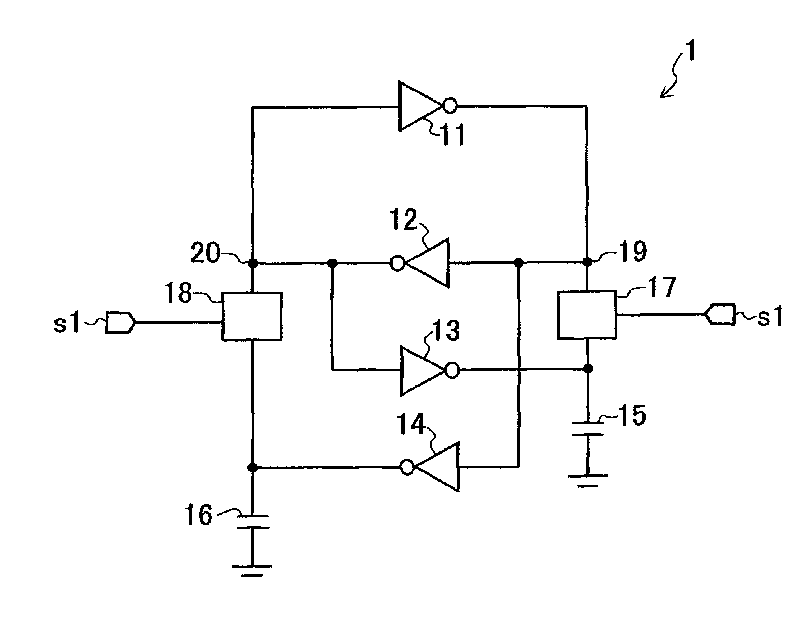
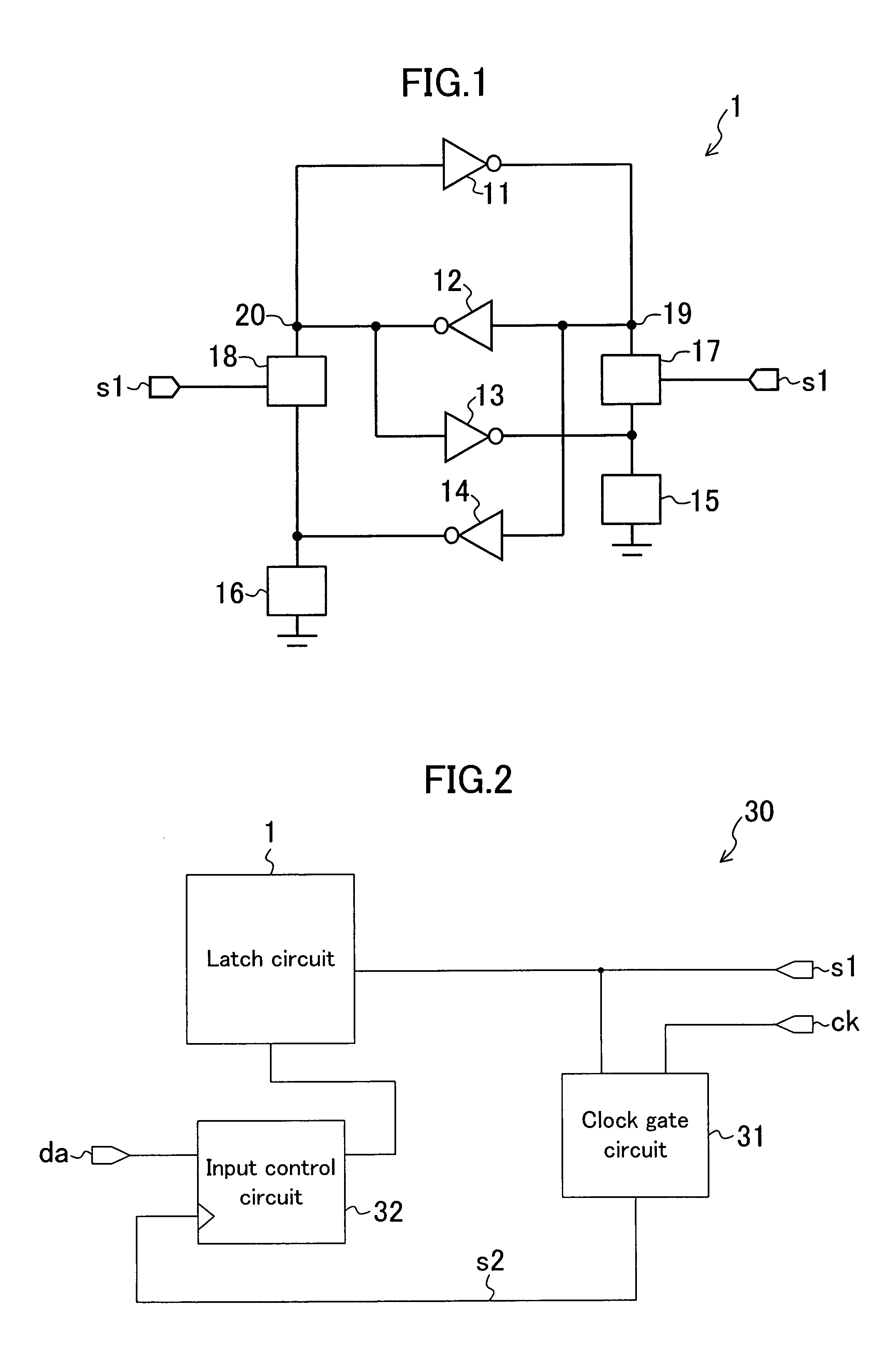
[0035]FIG. 1 shows an example of a configuration of a latch circuit according to a first embodiment. A latch circuit 1 includes inverter circuits 11, 12, 13, and 14, capacitor elements 15 and 16, and switching elements 17 and 18. The latch circuit 1 holds data in storage nodes 19 and 20 serving as connection points of the inverter circuit 11 and 12 which are cross-connected to each other. A configuration to hold data is not limited to the above configuration.

[0036]The inverter circuits 13 and 14 receive outputs from the inverter circuits 12 and 11, logically invert the outputs to output the logically inverted outputs, respectively. The inverter circuits 13 and 14 may be tristate inverter circuits (see, FIG. 13). In the tristate inverter circuit, an output can have a high impedance. For this reason, charging / discharging at the output terminal of the tristate inverter circuit can be suppressed, and a power consumption can be reduced.

[0037]The capacitor elements 15 and 16 are connected...

second embodiment

[0046]FIG. 2 shows an example of a configuration of a semiconductor integrated circuit according to a second embodiment. A semiconductor integrated circuit 30 includes the latch circuit 1 described above, a clock gate circuit 31, and an input control circuit 32.

[0047]The clock gate circuit 31 receives the control signal s1 of the switching elements 17 and 18 to control the presence / absence of outputting of an input clock signal ck on the basis of the control signal s1. In other words, by a control signal used in clock gated, the switching elements 17 and 18 are controlled. The input control circuit 32 controls the presence / absence of inputting of a data signal da to the latch circuit 1 in synchronism with an output signal s2 from the clock gate circuit 31. More specifically, the logical level of the signal s1 is set at “H” to instruct the discontinuation of the clock signal ck. At this time, since the clock gate circuit 31 transmits the clock signal ck, the input control circuit 32 ...

third embodiment

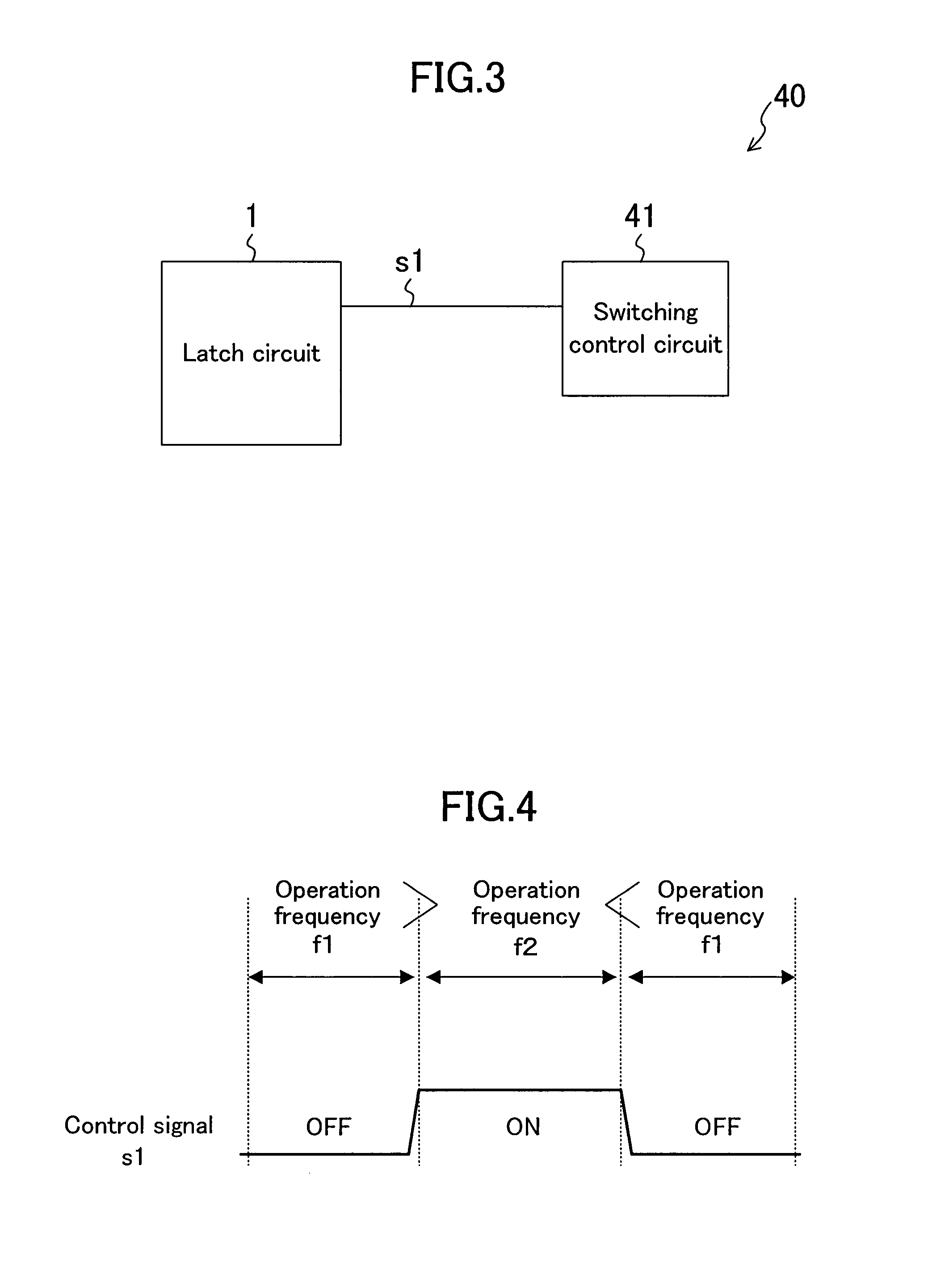
[0049]FIG. 3 shows an example of a configuration of a semiconductor integrated circuit according to a third embodiment. A semiconductor integrated circuit 40 includes the latch circuit 1 described above and a switching control circuit 41. The switching elements 17 and 18 are controlled by a control signal s1 output from the switching control circuit 41. An example of control of the semiconductor integrated circuit according to the embodiment will be described below.

First Example Of Control

[0050]FIG. 4 shows a first example of control of the latch circuit 1. The switching control circuit 41 sets the logical level of the control signal s1 at “H” when an operation frequency of the latch circuit 1 is switched from f1 to f2, and controls the switching element to an ON state. On the other hand, when the operation frequency of the latch circuit 1 is switched from f2 to f1, the switching control circuit 41 sets the logical level of the control signal s1 at “L” to control the switching eleme...


PUM


Abstract

A latch circuit includes first, second, and third inverter circuits, a switching element, and a capacitor element. The first inverter circuit and the second inverter circuit are cross-connected to each other. The third inverter circuit logically inverts an output from the first inverter circuit. The switching element is connected between the output terminal of the second inverter circuit and the output terminal of the third inverter circuit. The capacitor element is connected between the output terminal of the third inverter circuit and a reference voltage node.

Description

BACKGROUND OF THE INVENTION[0001]1. Field of the Invention[0002]The present invention relates to a latch circuit, in particular, a technique which stably holds data in a latch circuit.[0003]2. Description of the Related Art[0004]In a conventional circuit such as an SRAM or a cache which is required to be highly integrated, data breakdown caused by an α radiation, a neutron radiation, or the like is viewed as a problem because the capacitance of a storage node is small. This problem is called a soft error. On the other hand, a latch circuit has a storage node having a relatively large capacitance, the soft error is not viewed as a serious problem up to now. However, with miniaturization of recent semiconductor devices, the capacitance of a storage node in a latch circuit tends to decrease, and resistance to a soft error is necessarily improved even in the latch circuit.[0005]From a viewpoint of reduction in power consumption, a countermeasure such as a reduction in drive voltage is t...

Claims


Application Information

Patent Timeline
Patent Type & Authority Patents(United States)
IPC IPC(8): H03K3/00
CPCH03K3/356113H03K3/013
Inventor FUKUOKA, KOUHEI
Owner PANASONIC CORP
Why Eureka
Try Eureka